Thank you very much for your help,
I'm also interested in making diy speakers I will join the speakers forum, I like multiway speakers, do you know what I should read to start, do you recommend me any design in particular to start with? I don't know much about speakers. I don't know how to implement the passive crossover filter.
PS:
I will test your design with my amplifier.
Best regards,
Daniel Almeida
Hi Daniel,
I have an old copy of "Loudspeaker Design Handbook,4th edition" from Vance Dickason.
Take a look at kits from Madisound, but they can get very expensive however
The Madisound Speaker Store
It is so hard to give advise for speakers, because of so many options/prices
I have thread going discussing some old speakers I want to re-furbish, have a read.
http://www.diyaudio.com/forums/mult...fer-replacement-existing-box.html#post3697578
Cheers
Rick
Hi everyone,
I've made a few changes in my design to improve stability, but I'm concerned about two things, the phase shift cause by the input decoupling capacitors (inverting and noniverting inputs) are causing a phase shift of almost 180º at low frequencies (< 20 Hz) this can cause motorboating or similar humming oscillations?
The other thing that concerns me is a thermal stability problem that I have, because VAS current changes between 10.8 and 7.8 mA (0 to 100ºC), what can I do to have less variation, this variation could lead to problems?
It was told me that I should thermally compensate the drivers but I don't know how to do that because it's package is TO-92, any suggestions?
PS:
I'm using a compensation scheme that I call BTMC, to have more phase margin at 1kHz- 20kHz region what do you think about that?
Best regards,
Daniel
Attachments
Hi Daniel ,
Apologies for the delay in responding; I’ve been on holiday.
The C1R5 network is indeed an attempt to utilise the increased power dissipation afforded by a pulsed signal. Quite what this offers is difficult to determine for this device since no pulse response curves are shown. The time constant of 33ms was just a ball park figure, but is not too unrepresentative, given that Bob Cordell suggests a TC of 50ms as a figure for “illustrative purposes”. It can, of course, be removed entirely without any impact on the VI limiter values given. Note that it is not intended to alleviate any oscillation problems that might arise due to the switching of the protection transistor.
With a value of 10k for R5, it’s possible for a reasonably sized non-electrolytic to be used for C1.
Perhaps a higher gain device than 2N5551 if “base starvation” is an issue?
You have the spreadsheet. Try modifying it to suit your device parameters, then see how reactive loads fit.
Brian.
Hi everyone,
Thank you very much for your help Pingrs,
So do you think it's better to use the C1R5 network?
I think I have more oscillations when using this network, with lower values for R5 of course, I can't use 10 kohm with the 2N5551/2N5401 pair. What is the transistor model do you recommend me to use?
I'm sorry but I don't know how to use the spreadsheet.
Best regards,
Daniel
Daniel,
I would certainly add them to the pcb layout; you don't have to use them.
You're already using suitable transistors such as BC337C or BC560C, they will do.
I seem to remember a Leach constructor having oscillation problems in that region. He added a 10nF cap across one of the R3's at each side.
Brian.
Hi everyone,
Thank you very much for your help Pingrs,
So I can reduce the oscillations at the VI limiter if I put a capacitor across R3?
I've also seen base to collector capacitors, what do you think about that?
I think it's time to start making the PCB layout for my amplifier, do you think that I can use Eagle 6.3?
I don't know much about PCB layout for power amplifiers, this is my first solid state project, do you recommend me any reading?
I will try to do something until the end of this week and then I will post it.
Best regards,
Daniel
Daniel,
Take a look at this thread, they are working on finalizing this design
with what looks like two different layouts of the same schematic.
http://www.diyaudio.com/forums/solid-state/243481-200w-mosfet-cfa-amp-24.html#post3698456
@nattawa shows that he has done a few of them before.
Good layout means understanding the pcb fab process, the design/fabrication rules.
EIA/IPC is a group that define pcbs deaign/mfg standards.
Rick
Hi rsavas,
Thank you for repplying,
I will take a look at 200W MOSFET CFA amp PCB designs.
I should make the PCB with 2 or 4 layers?
I don't know the design/fabrication rules imposed by EIA/IPC.
Where I can consult those rules?
This amplifier is intended for personal use not for be made in large scale.
Best regards,
Daniel
Last edited:
2 layers is all that is necessary. Most of the old Japanese stereo's are 1-layer with the odd jumper.
You can refer to old Pioneer service manuals for guidance. get a login for hifiengine.com and download the Pioneer SX-1250/Spec-4 designs and see how they designed their stereos.
Use 10-12 mil min spacing rule and a finished hole to pad size rule
pad = finished hole 20 mil + 20 mil = 40mil
You are doing a power design so you want wide traces and copper fills for large current in ther o/p stage.
See
Futurlec.com - Printed Circuit Boards - Technical Information
I have not used these guys yet but am planning too.
Hi rsavas and thank you for your great help,
Do you think that I should do both channels (the amplifier is stereo) in the same PCB or I should make two PCBs?
The preamplifier and other tone controls must stay in this main PCB(s) or in another one, what about the power supply bridge rectifier and capacitors?
I will use this relays, how I can simulate the optocoupler before adding them to the PCB, I wanted to simulate this relay with the optocoupler, how I can simulate this circuits in LTSpice?
ESP - MOSFET Solid State Relays
Best regards,
Daniel
Up to you/ I guess that it depends on the size.Do you think that I should do both channels (the amplifier is stereo) in the same PCB or I should make two PCBs?
That I do not know.I will use this relays, how I can simulate the optocoupler before adding them to the PCB, I wanted to simulate this relay with the optocoupler, how I can simulate this circuits in LTSpice?
Need help!!!
Hi everyone,
I can't begin the PCB design right now because I still have some problems and doubts,
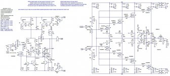
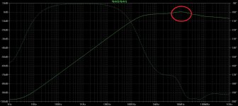
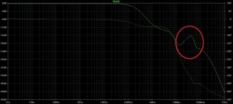
The main problem is that it seems that I've instabilities in internal nodes, I've added a few pictures about the strange responses of those nodes, even at the output there's a peaking starting at about 200 MHz.
The other problems are related to the current sources that are varying too much with temperature and the fact that I don't have thermal compensation for the drivers.
I don't know how to simulate an NTC thermistor in LTSpice and I want to simulate the thermal shutdown circuit, now that I've the output solid state relay, I also want to add a poping prevention delay network to connect also to the output relay, how I can connect all those things to the output relay with an OR logic gate?
The solid state relay I'm using is based on Rod Elliot's designs ESP - MOSFET Solid State Relays
Do you have some ideas about the startup delay circuit?
I really need your help, I can't move on with this project and make the PCB without achieving stability in the simulations.
I also need help with the stability problems, it's very important it's making me mad, because the amp has good gain/ phase margins but seems to have strange behaviours in the internal nodes. Why?
Please someone help me here!!
Thank you very much for your attention,
Best regards,
Daniel
Hi everyone,
I can't begin the PCB design right now because I still have some problems and doubts,
The main problem is that it seems that I've instabilities in internal nodes, I've added a few pictures about the strange responses of those nodes, even at the output there's a peaking starting at about 200 MHz.
The other problems are related to the current sources that are varying too much with temperature and the fact that I don't have thermal compensation for the drivers.
I don't know how to simulate an NTC thermistor in LTSpice and I want to simulate the thermal shutdown circuit, now that I've the output solid state relay, I also want to add a poping prevention delay network to connect also to the output relay, how I can connect all those things to the output relay with an OR logic gate?
The solid state relay I'm using is based on Rod Elliot's designs ESP - MOSFET Solid State Relays
Do you have some ideas about the startup delay circuit?
I really need your help, I can't move on with this project and make the PCB without achieving stability in the simulations.
I also need help with the stability problems, it's very important it's making me mad, because the amp has good gain/ phase margins but seems to have strange behaviours in the internal nodes. Why?
Please someone help me here!!
Thank you very much for your attention,
Best regards,
Daniel
Attachments
-
Cordell Models.txt19.2 KB · Views: 46
-
Amp7_btmc_hb5_s_bd12_prot_solid_state_output_relay.asc30.5 KB · Views: 64
-
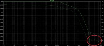 amp7_12_vout_instability.jpg298.2 KB · Views: 80
 -
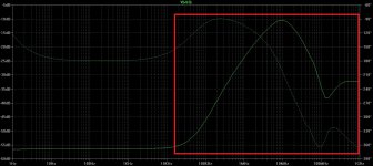 amp7_12_vb3_instability.jpg299.6 KB · Views: 180
 -
 amp7_12_vb2-vb1_instability.jpg300.6 KB · Views: 174
 -
 amp7_12_vb2_instability.jpg296.5 KB · Views: 179
 -
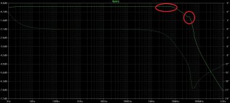 amp7_12_vb1_instability.jpg293.1 KB · Views: 197
 -
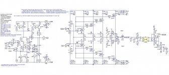 Amp7_btmc_hb5_s_bd12_prot_solid_state_output_relay.jpg193.7 KB · Views: 207
 -
BC3x7_40 Models.txt1.2 KB · Views: 44
- Status
- This old topic is closed. If you want to reopen this topic, contact a moderator using the "Report Post" button.
- Home
- Amplifiers
- Solid State
- How to make a low distortion lateral MOSFET amplifier?