Hi everyone,
Thank you very much for your help astx, I will download your models astx, and I will to take a look at the SOA discussions of your design.
I've already the Michael Kiwanuka's SOA papers, I'm thinking about a dual slope VI limiter like the one on figure 41, it's a good idea?
I will try to trace the curves on LTSpice.
PS: Q15/Q16 are the cascode transistors of the IPS (TCS), not EF pair, do you think my EF pair is unstable? I should add something to become stable?
Zobel network from gate to drain, or from base to collector, are a method to gain stability at higher frequencies (> 10-15 MHz), but degrades the phase margin very much, I had it included in my project, but I've removed them because of this problems
Now I use another method, base and gate stopper resistors to do a similar effect, they reduce the bandwidth of the transistor to the order of a few MHz (1-10 MHz), because they do a zobel network against Cpi/Cgs, they also introduce some phase lag, but it's acceptable.
Best regards,
Daniel
Attachments
Last edited:
Lowest THD figures using a single or dual slope VI limiter is nearly impossible. You have to decide: lowest THD or highest amplifier safety.I've already the Michael Kiwanuka's SOA papers, I'm thinking about a dual slope VI limiter like the one on figure 41, it's a good idea?
IMHO these are also EFs and may oscillate.PS: Q15/Q16 are the cascode transistors of the IPS (TCS), not EF pair, do you think my EF pair is unstable? I should add something to become stable?
BR, Toni
Hi everyone, and thank you for your help astx
I think that Q15/Q16 are common base, not EF (emitter-followers), because the constant voltage source is at the base and the signal enters the emitter and exits by the collector, creating some voltage gain, but no current gain (Ai = beta/(beta+1)), correct me if I'm wrong, please.
In an emitter follower (common collector), the constant voltage source is at the collector and the signal enters the base and exits by the emitter, this topology is a current amplifier, without voltage gain (Av aprox. 0.9-0.99), Ai = beta+1.
In a common emitter the constant current source is at the emitter and the signal enters the base and exits by the collector, this amplifier has both voltage and current gain, Av aprox [(-gm*Rc)/Re)], and Ai = beta.
PS:
As about the EF I've made with MJE15032 and MJE15033 it is stable?
I really want a dual-slope VI limiter, I expect that THD figures can get worse, but that's not a big problem, the amplifier should survive to real world conditions, like shorts and overloads.
If you want to make an amplifier similar to this one or based on this one (with the low THD figures presented), you can skip the VI limiter, and use fuse protection, or current limiting at the power supply.
Best regards,
Daniel
Last edited:
Hi everyone,
I'm sorry in common base Av = gm*Rc, and in common emitter Av aprox (Rc/Re), if Rc*gm >> 1.
I really wanted to make the SOA curves for the output stage, to incorporate the figure 41 circuit of Michael Kiwanuka's papers, can anyone help me here?
I know that this can be made using LTSpice, but I don't know the commands, I've looked at the astx amplifier SOA discussions and there are very valuable information there, but I don't what LTspice commands I should use to draw the SOA curves.
Best regards,
Daniel
Attachments
Last edited:
Hi everyone,
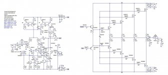
I've replaced the simple current mirror at the VAS by an improved current mirror, THD1 characteristics remain the same, THD20 characteristics are 10 ppm better, do you think that this change is a good idea?
And about the resistors at base of the TCS/TIS cascode transistors are a good or bad idea?
Best regards,
Daniel
Attachments
Hi everyone,
I've made a few more changes:
- I replaced the VAS 2N5551 for a BC550
- I replaced the Vbe multiplier for a BC550
Now simulated THD20 figures at 100W/8R and 200W/4R are both of less than 0.004 % and THD1 figures are of less than 0.00003 % for the 8 ohm load and less than 0.00004 for the 4 ohm load
What's your opinion about this changes?
I'm a little concerned about the output stage because I'm not thinking in incorporate zobels (base to collector or gate to drain) due to the increased phase lag that they introduce. So do you think that the base/gate stopper resistors are sufficient, they cutoff for -3dB at less than 5 MHz at the predrivers and less than 1 MHz at the output MOSFETs. This can be safe?
Best regards,
Daniel
Attachments
Last edited:
Hi everyone,
Thank you very much for your suggestions, I appreciate your help.
I could try the MJE15034/35, with 100-110 mA if I has the LTSpice models for those transistors. Can you give me the models, please?
I'm really sorry mcd99uk, but I don't know what is a bootstrapped driver. Can you explain it to me, please?
Best regards,
Daniel
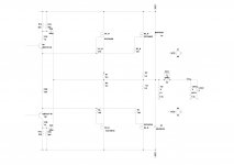
Here is an example of bootstrapped driver. Set Driver Bias current to around 5mA.
Set voltages at nodes where the 10R resistors meet the 5k6 nodes to about the max Vgs you want to allow. Changing the 5K6 resistors as well as changing the bias sets this voltage.
Using this method means you don't need gate zeners.
Set voltages at nodes where the 10R resistors meet the 5k6 nodes to about the max Vgs you want to allow. Changing the 5K6 resistors as well as changing the bias sets this voltage.
Using this method means you don't need gate zeners.
Attachments
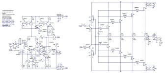
Hi everyone,
Thank you very much mcd99uk, this bootstrapped predriver arrangement really lowers THD1 and THD20, now I have this THD1 values of less than 15ppm at 200W/4R and 100W/8R
I'm only using 100 ohm base stopper resistors to prevent parasitic oscillations at the predriver EF, do you think that I should use a larger value for base stopper resistors, or a base zobel network?
I'm using 2N5551/2N5401 as the bootstrapped predrivers, with 5 mA current, and 12 V Vgs limiting. I should use the BCs? If so can you give me the models, please?
PS: As the 2N5551/2N5401 have lower junction capacitances, I have less phase lag and so more phase/gain margin than before (68º->72º, 11->12 dB).
Best regards,
Daniel
Attachments
Last edited:
You can find models for BC3x7-40 devices here. Check out the SOA @ 12V. More than enough. The -40 rank have very good hfe.
http://www.diyaudio.com/forums/solid-state/243481-200w-mosfet-cfa-amp-9.html#post3657020
Also, consider adding a resistor in series with the "speed up" cap. I had oscillation problems without it. Just use a very low value as a "place holder" to remind you to leave a space if you design a pcb.
Edit: I don't like those MJE devices at all. Too slow. I avoid them at all costs unless that sort of capacity is really required. Also, 100R base stoppers should be fine as long as your PCB layout is sensible. I have only used 10R on my amp.
BC5x0c's work well too in this application.
Last edited:
Danny.
Look at your Output Thiele Network.
The first R+C looks about right using 100n and 10r. This must be located right next to the output stage and the Power Ground right next to the output stage.
The R//L looks wrong. 10r//1u is usually insufficiently damped. Try 1r to 5r //1u
The last R+C looks wrong. 10r + 100n does not drop the RF attenuation low enough. Try 2r to 6r.
This last R+C must be across the speaker terminals. To attenuate the RF attempting to get inside the chassis. Both terminals can be shunted to Chassis with 1nF ceramic.
I have found that the R of the R//L and the R of the last R+C should total approximately the nominal load impedance. i.e. for 8ohms speakers 3r//0.7uH and 5r+68nF give 8r+68nF at VHF. For 4ohms, try ~1r5//1uH & 2r4+100nF
This (8ohms) is then in parallel with the 10r+47nF from the output stage to give a net 4r5+115nF as the total VHF load.
The 6m8F on the feedback leg is going to take a long time to charge and stabilise. You may have to use a long time delay with your speaker relay.
Unusual combination of RF input filter values.
Add a low pF NP0 ceramic to shunt the signal to Chassis at the input socket. The 2n2F will not be effective at uhf.
Hi everyone, and thank you mcd99uk, and andrewT for your help,
What about using BC550/BC560 pair as bootstrapped drivers, good idea?
Do you think I should use a lower Vgsmax voltage?
The bootstrapped drivers are more prone to oscillations than the common EF pair?
If so I will think twice before using one.
Are you sure that your oscillation problem isn't caused by lower base stopper resistors, with 10R you have higher frequency cuttof (I think it is of 800 MHz), with 100R you have a low frequency cutoff of 80 MHz, even though, I think I should use a larger resistor value if I use the BCs (maybe 220R or 330R). I'm assuming that Ciss aprox Cje but I think that this might be wrong.
About the output Thiele network, input and feedback networks, I will look at them latter and will reply to you, AndrewT. Thank you for help me with this problems
What I should do if the amp are build to be used either with 8 or 4 ohm speakers?
Best regards,
Daniel
Last edited:
Hi everyone,
I need help here!!!
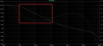
I've been reading vostro's thread about compensation and stability and I found out that this amplifier might be unstable. All my work could be worthless!!! Because I've less than 8 degrees PM (with bootstrapped drivers), less than 14 degrees PM (without bootstrapped drivers) at 10 kHz like in vostro's amp, and that's a danger sign, I can't achieve much higher PM levels using TPC/TMC even using higher capacitor values, the maximum I've got is 15-20 degrees, much less than the minimum 45 degrees allowed. Please I need help. All my work could be done in vane if the compensation scheme doesn't work properly.
PS: It's rare to see an amp using TMC/TPC with more than 10-15º at 10 kHz, why?
Is this a sign that TPC/TMC are very unstable compensation scheemes?
I really need help here
Best regards,
Daniel
I need help here!!!
I've been reading vostro's thread about compensation and stability and I found out that this amplifier might be unstable. All my work could be worthless!!! Because I've less than 8 degrees PM (with bootstrapped drivers), less than 14 degrees PM (without bootstrapped drivers) at 10 kHz like in vostro's amp, and that's a danger sign, I can't achieve much higher PM levels using TPC/TMC even using higher capacitor values, the maximum I've got is 15-20 degrees, much less than the minimum 45 degrees allowed. Please I need help. All my work could be done in vane if the compensation scheme doesn't work properly.
PS: It's rare to see an amp using TMC/TPC with more than 10-15º at 10 kHz, why?
Is this a sign that TPC/TMC are very unstable compensation scheemes?
I really need help here
Best regards,
Daniel
Attachments
Last edited:
Hi everyone,
I need help here!!!
I've been reading vostro's thread about compensation and stability and I found out that this amplifier might be unstable. All my work could be worthless!!! Because I've less than 8 degrees PM (with bootstrapped drivers), less than 14 degrees PM (without bootstrapped drivers) at 10 kHz like in vostro's amp, and that's a danger sign, I can't achieve much higher PM levels using TPC/TMC even using higher capacitor values, the maximum I've got is 15-20 degrees, much less than the minimum 45 degrees allowed. Please I need help. All my work could be done in vane if the compensation scheme doesn't work properly.
PS: It's rare to see an amp using TMC/TPC with more than 10-15º at 10 kHz, why?
Is this a sign that TPC/TMC are very unstable compensation scheemes?
I really need help here
Best regards,
Daniel
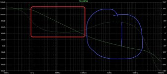
You looked at the wrong place. Where the gain crosses the zero you have to look for phase margin.
Attachments
Thank's a lot dadod, so I have sufficient phase/gain margins, sorry for my confusion
PS:
That lack of phase margin characteristic of TPC/TMC (which are related - Michael Kiwanuka demonstrated it) at that low frequencies can be a sign of danger?
I personally think that no because the Barkhausen criterion for self sustaining oscillation is not met, that is phase = 0 arround the loop, and (feedback x open loop gain) product module = 1 (0dB)
Last edited:
Thank's a lot dadod, so I have sufficient phase/gain margins, sorry for my confusion
PS:
That lack of phase margin characteristic of TPC/TMC (which are related - Michael Kiwanuka demonstrated it) at that low frequencies can be a sign of danger?
I personally think that no because the Barkhausen criterion for self sustaining oscillation is not met, that is phase = 0 arround the loop, and (feedback x open loop gain) product module = 1 (0dB)
There is no problem, phase can come close to 180 degree(but not crossing it) and an amp with TPC/TMC compensation is very stable. I am listening one each day with no stability problem at all.
Hi everyone,
Talking about the bootstrapped drivers again, this arrangement in fact lowers THD, and dispenses the use of gate zeners but it is more prone to HF oscillations than the common EF pair?
What do you think?
I could put a resistor in series with the speedup capacitor like mcd99uk, but if I do that I will add a filter to the circuit, is this a good idea?
The speedup capacitor is the one I refer to as Cbypass2, right?
In fact that capacitor could cause oscillations, because there is an EF driving a capacitive load
I can simply throw Cbypass2 away?
The increase in THD20 is almost insignificant.
As about the bootstrapped driver transistors I could use BC550/560 pair?
Best regards,
Daniel
Attachments
Last edited:
- Status
- This old topic is closed. If you want to reopen this topic, contact a moderator using the "Report Post" button.
- Home
- Amplifiers
- Solid State
- How to make a low distortion lateral MOSFET amplifier?