I have previously shown that an amplifier with TPC possesses exactly the same major loop gain across the audio band as the total loop gain enjoyed by the second stage and the output stage alone with so-called "TMC" provided the same compensation elements are used in both cases.
This proves that TPC and "TMC" are, in fact, two sides of the same coin, and that "TMC" is merely TPC localised to the second stage and the output stage.
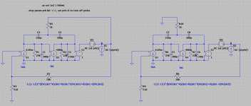
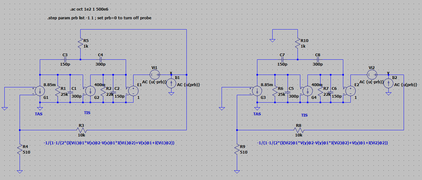
In order to characterise the major loop transmission of TPC with respect to the transmission of the minor loop about the output stage with "TMC" (in the presence of the major loop) outside the audio band, a second order model of the generic (Thompson) amplifier is used. This consists of a differential voltage controlled current source for the input (transadmittance) stage (TAS) driving a transimpedance stage (TIS) whose two uncompensated dominant poles are modeled by a parallel RC network at its input and output.
This second order model is preferred to previous demonstrations in which real transistors were used because it excludes extraneous singularities from the system, and, therefore, permits the isolation of those singularities that are intrinsic to the two compensation methods.
The attached extract from a yet-to-be-published paper of mine explains how the second order model works.
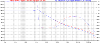
From the attached graph, it is apparent, as explicated above, that the total loop gain (in the audio band and up to 100KHz) about the second stage and the output stage with "TMC" (red trace) is exactly the same as the major loop gain with TPC (blue trace).
Secondly, it is clear that the initial double-pole roll-off with TPC reverts, as expected, to a single pole roll-off due to the introduction of a zero, and that the same zero also obtains in the "TMC" minor loop. With the latter it is also apparent that the zero is closely followed by a zero-pole doublet. These three singularities together have the net effect of causing the response of the "TMC" minor loop to appear in parallel with that due to the major loop with TPC at frequencies beyond those of their common dominant zero.
Clearly, a stable "TMC" loop can be realised by merely calculating the component values required to give a stable major loop with TPC, and then simply connecting the TPC resistor to the output to give a stable "TMC" compensator.
Caution must, of course, be exercised to ensure that the slightly greater unity loop transmission frequency of the "TMC" minor loop (compared to that of the TPC major loop) doesn't compromise stability of the loop.
This proves that TPC and "TMC" are, in fact, two sides of the same coin, and that "TMC" is merely TPC localised to the second stage and the output stage.
In order to characterise the major loop transmission of TPC with respect to the transmission of the minor loop about the output stage with "TMC" (in the presence of the major loop) outside the audio band, a second order model of the generic (Thompson) amplifier is used. This consists of a differential voltage controlled current source for the input (transadmittance) stage (TAS) driving a transimpedance stage (TIS) whose two uncompensated dominant poles are modeled by a parallel RC network at its input and output.
This second order model is preferred to previous demonstrations in which real transistors were used because it excludes extraneous singularities from the system, and, therefore, permits the isolation of those singularities that are intrinsic to the two compensation methods.
The attached extract from a yet-to-be-published paper of mine explains how the second order model works.
From the attached graph, it is apparent, as explicated above, that the total loop gain (in the audio band and up to 100KHz) about the second stage and the output stage with "TMC" (red trace) is exactly the same as the major loop gain with TPC (blue trace).
Secondly, it is clear that the initial double-pole roll-off with TPC reverts, as expected, to a single pole roll-off due to the introduction of a zero, and that the same zero also obtains in the "TMC" minor loop. With the latter it is also apparent that the zero is closely followed by a zero-pole doublet. These three singularities together have the net effect of causing the response of the "TMC" minor loop to appear in parallel with that due to the major loop with TPC at frequencies beyond those of their common dominant zero.
Clearly, a stable "TMC" loop can be realised by merely calculating the component values required to give a stable major loop with TPC, and then simply connecting the TPC resistor to the output to give a stable "TMC" compensator.
Caution must, of course, be exercised to ensure that the slightly greater unity loop transmission frequency of the "TMC" minor loop (compared to that of the TPC major loop) doesn't compromise stability of the loop.
Attachments
Last edited:
Caution must, of course, be exercised to ensure that the slightly greater unity loop transmission frequency of the "TMC" minor loop (compared to that of the TPC major loop) doesn't compromise stability of the loop.
Doesn't your simulation show the TMC with substantially BETTER PhaseM than the TPC, despite the small increase in cross-over frequency?
1/3 radian is not trivial.
Best wishes
David
"TMC" shows some fifteen degrees better phase margin at unity minor loop gain frequency because it has two dominant zeros following the dominant coincident poles.
Note, however, that this is not necessarily an advantage as the unity minor loop gain frequency with "TMC" is nearly an octave higher than that due to the major loop with TPC.
You can establish this yourself by running the simulation; I attached the .asc file to the introductory post.
Note, however, that this is not necessarily an advantage as the unity minor loop gain frequency with "TMC" is nearly an octave higher than that due to the major loop with TPC.
You can establish this yourself by running the simulation; I attached the .asc file to the introductory post.
These two circuits:
have identical connectivity, and identical component values. Additional trace loop appears in left hand circuit. Does simulation account for trace length, and loop area? Loops existence in simulation may change calculations due to additional node with differences in results plots >100kHz strictly due to differing number of round off errors.
All I see here is modeling error of two identical circuits.
These two circuits have identical connectivity, and identical component values. Additional trace loop appears in left hand circuit. Does simulation account for trace length, and loop area? Loops existence in simulation may change calculations due to additional node with differences in results plots >100kHz strictly due to differing number of round off errors.
All I see here is modeling error of two identical circuits.
No. These two circuits have identical component values, but, self-evidently, NOT identical connectivity.
No. There is no "modelling error of two identical circuits".
Of course simulation does not "account for trace length and loop area". You've missed the point I fear. The purpose of simulation is to gain insight into circuit behaviour; in this case, the conduct of "TMC" with respect to TPC without consideration of extraneous third order singularities due to "trace length and loop area", and so on and so forth.
Last edited:
"TMC" shows some fifteen degrees better phase margin at unity minor loop gain frequency because it has two dominant zeros following the dominant coincident poles.
Note, however, that this is not necessarily an advantage as the unity minor loop gain frequency with "TMC" is nearly an octave higher than that due to the major loop with TPC.
Usually an increased loop crossover frequency is an issue because it impacts stability.
But in this case, despite the increase in frequency the TMC is a third of a radian better.
The resultant improvement in stability is what matters.
Well done on the post of the asc.
Best wishes
David
...
This proves that TPC and "TMC" are, in fact, two sides of the same coin, and that "TMC" is merely TPC localised to the second stage and the output stage.
...
I think I agree, but a major difference in a real circuit would be that the TPC load the VAS significantly more than a TMC do?
"The TMC is a bootstrapped TPC."
I think I agree, but a major difference in a real circuit would be that the TPC load the VAS significantly more than a TMC do?
I haven't seen any evidence that this is the case.
I haven't seen any evidence that this is the case.
Hi,
It looks to be the case to me. 1K to ground and 1K
bootstrapped from the output looks different loading.
Unless I'm missing something the current through the
1K will be lower for the bootstrapped case than ground.
Doug Self got slew rate limiting with TPC due to the
VAS not be able to drive the resistor to ground.
rgds, sreten.
Hi,
Doug Self got slew rate limiting with TPC due to the
VAS not be able to drive the resistor to ground.
rgds, sreten.
If I am not mistaken, D. Self did not get slew limiting with TPC "due to the VAS not be able to drive the resistor to ground". I think he said there was a slight increase in HF distortion due to such loading.
However, his findings were true only for the case where the capacitor connected to the TIS output is significantly larger than that connected to its input.
I think I agree, but a major difference in a real circuit would be that the TPC load the VAS significantly more than a TMC do?
The thoughts below may be completely wrong...
It does look like (to me) TPC loads the VAS output more but could this be negated by moving the TPC connection to the next stage (eg. drivers or pre drivers). But this may well require extra compensation as TPC compensation now encloses more transistors? And then the advantage of moving the TPC "take off point" may be reduced?
If I am not mistaken, D. Self did not get slew limiting with TPC "due to the VAS not be able to drive the resistor to ground". I think he said there was a slight increase in HF distortion due to such loading.
However, his findings were true only for the case where the capacitor connected to the TIS output is significantly larger than that connected to its input.
Hi,
Check your references. A significant increase in distortion at h.f.
due to assymetrical current clipping in the Vas with a resistor of
far higher value than you suggest, and similar capacitance ratio.
The point made is very valid, and is not to be dismissed IMO.
rgds, sreten.
Your model does not seem to include the very real effect.
Last edited:
Your model does not seem to include the very real effect.
I did not use the model to check the current draw of the various elements of the compensation networks on the TIS.
However, this is easily done by deleting the loop gain probes, replacing the SPICE directives with those for transient analysis at some high frequency of your choice and introducing an AC source at the input of each of the models.
Comparing the currents drawn by the compensation elements should enable you to compare the loading effects on the TIS of the two compensation networks.
For a more realistic simulation in this instance use a circuit using "real" transistors.
Last edited:
The thoughts below may be completely wrong...
It does look like (to me) TPC loads the VAS output more but could this be negated by moving the TPC connection to the next stage (eg. drivers or pre drivers). But this may well require extra compensation as TPC compensation now encloses more transistors? And then the advantage of moving the TPC "take off point" may be reduced?
To reduce the current draw of the TPC network on the TIS, simply swap the capacitors so that the larger capacitor is connected to the input of the TIS, while the larger of the two is connected to its output.
Including the output stage driver in the compensation loop is likely to require compensation of the minor loop by means of a shunt RC network at the output of the second stage. This, as you've observed, is generally the case where more than two transistors are enclosed within the minor loop.
The Bang and Olufsen Beocenter 7000 compact stereo amp part
has a 47pF miller capacitor that goes from VAS input straightly to the
power stage output through a 270R and there s no added shunt compensation
for the second stage , only a lead compensation from output to inverting input
as well as a shunt at the IPS output ,so it depend ultimately of the practical
implementation ; i guess that there s more than a way to Rome..
I did not use the model to check the current draw of the various elements of the compensation networks on the TIS.
However, this is easily done by deleting the loop gain probes, replacing the SPICE directives with those for transient analysis at some high frequency of your choice and introducing an AC source at the input of each of the models.
Comparing the currents drawn by the compensation elements should enable you to compare the loading effects on the TIS of the two compensation networks.
For a more realistic simulation in this instance use a circuit using "real" transistors.
Hi,
That is IMO obfuscating something relatively simple.
VAS load current is not a complicated issue.
D. Self used about 10K for TPC, and still had problems
related to normal VAS current for driving the output.
rgds, sreten.
Use of not well known acronyms is just pointlessly tedious.
Is not remotely clever to not explain them when first used.
Last edited:
The thoughts below may be completely wrong...
It does look like (to me) TPC loads the VAS output more but could this be negated by moving the TPC connection to the next stage (eg. drivers or pre drivers). But this may well require extra compensation as TPC compensation now encloses more transistors? And then the advantage of moving the TPC "take off point" may be reduced?
From my simulations on my last amp I`ve found that if VAS is a double BC557C (darlington-like) the Ccb is enough to stabilize this stage if there is an additional miller from the output. If the collector of the first VAS-transistor is connected to ground it will go unstable without a miller-cap.
My next amp (if VF) will most likely be using a very small VAS-miller (a few pF) and a TPC from the output to VAS input.
Of course, the VAS Ccb is hardly linear and it might be a bad idea to use it in any feedback-loop.
...as well as a shunt at the IPS output...
Shunt compensation at the output of the input stage also helps stabilise the minor loop, but, I suspect, it compromises power supply rejection; further investigation is required in this respect.
Use of not well known acronyms is just pointlessly tedious. Is not remotely clever to not explain them when first used.
Just run a search of the acronym at issue on the forum. I haven't used an acronym yet that I haven't previously exhaustively and repeatedly elucidated.
- Status
- This old topic is closed. If you want to reopen this topic, contact a moderator using the "Report Post" button.
- Home
- Amplifiers
- Solid State
- Demonstrating that TPC and so-called "TMC" are related