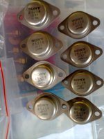
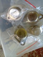
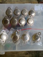
A friend gave me 4 pcs 2SK60 with rank JN-54 and I had purchased 2SJ18 with ranks JG-57, all OLD and Sony originals I think. I plan to use this for a Push Pull complimentary amp but when goggling around for Vfets and go on Sony TA-4650 service manual, there's a note in there saying that ...whenever replacing VFET they must be at the same rank else it will only cause destruction of the vfets. What i don't understand is, does it requires for all N and P channel vfets to be of the same rank ?
My Nch are all rank 54 and Pch are 57..the're not of the same rank so it can't be used on same time?
Another question is does this vfets needs to run on always on class A?
Can anybody show me schematics and enlighten me or guide me to where can i use this treasure SITs ?
My Nch are all rank 54 and Pch are 57..the're not of the same rank so it can't be used on same time?
Another question is does this vfets needs to run on always on class A?
Can anybody show me schematics and enlighten me or guide me to where can i use this treasure SITs ?
Attachments
A friend gave me 4 pcs 2SK60 with rank JN-54 and I had purchased 2SJ18 with ranks JG-57, all OLD and Sony originals I think. I plan to use this for a Push Pull complimentary amp but when goggling around for Vfets and go on Sony TA-4650 service manual, there's a note in there saying that ...whenever replacing VFET they must be at the same rank else it will only cause destruction of the vfets. What i don't understand is, does it requires for all N and P channel vfets to be of the same rank ?
My Nch are all rank 54 and Pch are 57..the're not of the same rank so it can't be used on same time?
Another question is does this vfets needs to run on always on class A?
Can anybody show me schematics and enlighten me or guide me to where can i use this treasure SITs ?
This is normally only an issue if you place several in parallel. In parallel circuitry the FETs have a common bias arrangement, so when their threshold voltage is not the same, the FETs in the parallel set will have different bias currents and they don't share the load very well.
The threshold voltage of the N- and P- channel devices does not have to be the same, as long as the bias circuit has enough adjustment range for the required bias current.
jan
Thanks Mr Didden....so I can still use this pair even in parallel since all my k60 is rank 54 and all my J18 is rank 57...I thought this is applicable for N and P pair....
They say that this Vfet's are Solid state triodes since it has similar characteristic with that of a triode .Does someone tried and prove it?
They say that this Vfet's are Solid state triodes since it has similar characteristic with that of a triode .Does someone tried and prove it?
They say that this Vfet's are Solid state triodes since it has similar characteristic with that of a triode .Does someone tried and prove it?
Like this?
Attachments
Like this?
Ilimzin , i expected this thread to make you exit from the woods.
")
Your comments on theses matters are always very interesting
and quite insightfull.
I do remember that the official Sony supplied repair kits for these amps did have N and P channel FET's of the same rank in each kit. As Jan mentions though, its not such an issue as long as each group of N and each group of P are similar.
Junm... you do realise these devices are like no other and they can not be "dropped into" conventional output stages.
Junm... you do realise these devices are like no other and they can not be "dropped into" conventional output stages.
This is normally only an issue if you place several in parallel. In parallel circuitry the FETs have a common bias arrangement, so when their threshold voltage is not the same, the FETs in the parallel set will have different bias currents and they don't share the load very well.
The threshold voltage of the N- and P- channel devices does not have to be the same, as long as the bias circuit has enough adjustment range for the required bias current.
Jan, although your statement is in general true, I will have to disagree with you in this particular instance. The reason is that the Sony rank system for VFETs does indeed indirectly map to treshold voltage, but other important parameters track the rank number, such as Idss and mu of the VFET.
Also, one should be aware that the rank number defines at which Vgs the drain current will be 100mA at Vds=50V (if memory serves me right). As you can see, the current the Vgs is defined for is quite high, and in fact this happens to be a typical bias current for a single J18/K60 VFET in a complementary power amp stage used in Sony units built around these VFETs. It is rather difficult to talk about it as a 'treshold voltage' in this sense. The coding of the rank number (only the last dgit is signifficant) is, as far as i have been able to deduce, 7.5 + (rank * 2.5) volts, and this is valid for ranks 3 to 7. There are ranks 1 and 2 which have a different definition but I won't go into that here.
Anyway, for a simple complementary output stage it would be advisable to have all paralleled VFETs be the same rank, and complements not to differ more than one rank number. This is if the simples biasing arrangement is used, and output symmetry is desired regarding transfer characteristic and clipping behavior. Lower rank units tend to have higher Rds. Now, at this point it has to be said that although VFETs/SITs in general are referred to as semiconductor triodes, there are differences in their characteristics just like there are different triodes, and various manufacturers went different ways when deciding how to make their SITs behave. Sony units are lower gm, lower capacitance units that are very linear (almost perfect triode, see graph above) at higher voltages. At low voltages all SITs tend to behave more like a variable resistor, and in most cases at Vgs=0 there is a definite resistor characteristic that does tend to have a knee of sorts and a saturation area but usually at currents higher than the maximum permissible limit. The Rds of Sony units is quite high and does depend on rank quite a bit. Further, although they are very linear at higher voltages, they are usually not used at those voltages (see graph in my previous post - it goes to Vds=240V!) so the normal mode of operation is a cross between triode and resistive behavior. Using complementary pairs that have a high rank difference will result in a rather asymmetrical transfer characteristic and also (assuming Vgs is at most zero) clipping will be asymmetrical because the maximum output voltage to load will be limited by Rds, which will be different for the positive and negative output voltage.
The asymmetry itself might have advantages as it will not cancel all even harmonics hence may sound more pleasing to the ear to some.
In any case a few important points are to be made for would-be designers of VFET amps:
1) It IS a triode. Hence, all terminals are inputs and drain current depends on both Vgs and Vds. This means that with changing power supply voltage (be that mains fluctuations or ripple) the bias current through a simple VFET complementary output stage changes when the bias voltage is constant. Exploring the available VFET amp schematics from the late 70s and early 80s will show that all had means implemented to compensate for this. One might think it's a moot point but given the high variability of the VFET characteristics between the same type, not taking care of this results in output (inter)modulation by the mains supply ripple, the more of it, the larget the difference between the P and N half of the output stage. Simplest way to get around it (and solve another problem) is to regulate the power supply for the output stage.
2) SIT/VFET history is that of a device designed for extremely fast switching speed, the linear behavior is a byproduct. All VFETs have a 'beta' mode, i.e. current amplification mode, where Vgs is positive and current flows from gate to source. In this mode the equivalent Rds falls dramatically (factor of 10 or more!) and this is used to get the switching behavior. The important bit for audio designers is that positive Vgs is also used to get peak output, without this the voltage losses on a VFET are very high (often at Vgs=0 peak dissipation is reached before the maximum output current for the device). That being said, the G-S 'diode' has a maximum limit on the current, so the current from the driver stage must be limited to a safe value. VFETs are EXTREMELY hard to kill compared to any other semiconductor I know off except maybe a bog standard rectifier diode. And, in most cases what happens is that the G-S diode is overloaded and blows it's bonding wire (the very thin wire going from the gate pin to the gate structure on the crystal)!
One thing which can be used to an advantage here is that already small positive Vgs decrease Rds substantially. A schottky diode in parallel to G-S of the VFET or even a regular diode and series resistor to G-S can be used to protect the VFET very effectively.
It should be noted that the transfer function for very low Vgs (including positive Vgs, this is limited to one dide drop as the G-S structure of a VFET is that of a junction FET, i.e. diode) is quite nonlinear and has a compression characteristic to it.
3) There is no optimum bias for VFETs, they are similar to MOSFETs in that regard. However, because of the generally low mu (voltage amplification factor) and triode character (which includes the cut-off or lack thereof characteristics) a push-pull output stage with VFETs has a very wide crossover region even at fairly low (for a VFET) bias current. The caharcteristics of these low gm VFETs at low voltages result in something like hyperbolic class AB operation where it's possible to set up biasing so that the halves of a push-pull stage never turn off completely, yet the total current from the power supply is not constant like in class A - the bias current can be much lower. In essence you get a 'high bias class AB' but without crossover from the positive and negative halves of the signal, like in class A.
So, as the original poster asked, no, just like any other element VFETs do not have to work in class A, unless they operate in a single-ended design, but the bias current is generally similar to that of MOSFET stages so standing dissipation will be higher. That being said, all the advantages of class A can be had at bias currents well below theoretical class A operation (that being 1/2 of the maximum output current). So, design for larger heatsinks
4) It is a depletion mode device, hence turned on with no bias. As I mentioned before, VFETs don't really have an Idss that can be defined like for small signal JFETs, but equivalent Rds is low enough at Vgs=0 to destroy a VFET if there is no bias present at output stage power up. With actual triodes this is usually taken care of by voltages being there before the cathode has heated up sufficiently for current to flow so no problem, but this is a semiconductor and it works instantly. Therefore, some means of assuring that the bias voltage comes up before the main output stage power supply voltage, must be included in the design. I mentioned above that a regulated output stage power supply solves an important problem for VFET output stages, and having one with a few extra parts also solves the problem of bias voltage needing to be present before the main power supply voltage for the output stage. In any case very simple circuits will offer excellent performance here - a simple one transistor voltage follower series regulator does wonders.
Ilimzin , i expected this thread to make you exit from the woods.
Your comments on theses matters are always very interesting
and quite insightfull.
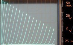
The graph is a composite of two graphs taken by a Tek curve tracer, this is a 2SK60 (don't remember the rank though but it could be decoded from the graph). There is one interesting thing to note here - 2SK60/2SJ18 were specified for max Vds up to 160 or 170V depending on where you get the (extremely scarce!) data. I have done measurements on... well, MANY VFETs of various kinds and I can state with certainty that they were all very much under-specified. Apparently the manufacturers wanted to be certain that the spec fits despite the large variances between parts of the same kind.
That being said I have yet to encounter a VFET that did not have a signifficantly higher Vdsmax compared to spec - most J18/K60 start showing leakage at well over 200V (usually 250-270V) and it usually happens not because of D-S breakdown but D-G breakdown, driving the G terminal positive and increasing conductance of the part. You can see that in the diagram above, the voltage goes to 240V and the part still shows expected behavior.
Note also the first few Id-Vds lines on the left - the very first one is for Vgs=0. At Id=500mA it already shows a couple of V Vds, so equivalent Rds is high. Also the curves (2V of Vgs apart) degrade to a resistor at low voltages.
High voltage curves show extreme linearity - it should be said that this is NOT a hallmark of any VFET - different manufacturers had different philosophy on how it was supposed to behave for best effect. Still, looking at the curves it's obvious that a standard transformer coupled SE output stage is not only possible but desirable if low distortion with no feedback is what one desires.
My Nch are all rank 54 and Pch are 57..the're not of the same rank so it can't be used on same time?
You might want to look for 2SJ18 rank 4 here:
SONY 2SJ18 TO-3 P-CHANNEL MOS FET FOR HIGH SPEED SWITCHING | eBay
However, have a look at the end of this post...
Another question is does this vfets needs to run on always on class A?
No, and normally it does not
Can anybody show me schematics and enlighten me or guide me to where can i use this treasure SITs ?
AMPLIMOS one stage amplifiers, amplificatori audio monostadio
Although, I would have a good look at the vintage gear schematics that used VFETs, and use most of the other ones as ideas. As someone pointed out, iff you only have semiconductor design experience regarding amplifiers, VFETs are like nothing you have ever worked with and require some attention not only to the 'housekeeping; circuits around them, but also to the best point and topology to use them in, to be used optimally. Manu of the schematic on that site show clear signs of their authors not completely understanding the issues around VFETs. However, if you have ever designed with tubes, triodes in particular, and have some knowledge of OTL designs, it will be of great help with VFETs.
I shall also add a warning here - there is a new 'fad' regarding fake parts lately (and mostly in China of course), which is re-marking atual genuine parts of some kind with markings for parts that sell. So, instead of getting what you want, you are getting a part that is genuine, and the right polarity, but all the rest is lottery.
VFET sources are scarce but there are some. One has rank 1 and 2 parts which are not compatible with old Sony amplifiers (without some mods) and it seems that these have also come under the busy little hands of the re-markers. I've had a bunch of Sony VFETs with fake markings and rank that does not correspond to the part. So, be careful when ordering. Check that the markings do not come off easily (fake ones will come off instantly with Isopropyl alcohol!).
Jan, although your statement is in general true, I will have to disagree with you in this particular instance. The reason is that the Sony rank system for VFETs does indeed indirectly map to treshold voltage, but other important parameters track the rank number, such as Idss and mu of the VFET.
Also, one should be aware that the rank number defines at which Vgs the drain current will be 100mA at Vds=50V (if memory serves me right). As you can see, the current the Vgs is defined for is quite high, and in fact this happens to be a typical bias current for a single J18/K60 VFET in a complementary power amp stage used in Sony units built around these VFETs. It is rather difficult to talk about it as a 'treshold voltage' in this sense. The coding of the rank number (only the last dgit is signifficant) is, as far as i have been able to deduce, 7.5 + (rank * 2.5) volts, and this is valid for ranks 3 to 7. There are ranks 1 and 2 which have a different definition but I won't go into that here.
Anyway, for a simple complementary output stage it would be advisable to have all paralleled VFETs be the same rank, and complements not to differ more than one rank number. This is if the simples biasing arrangement is used, and output symmetry is desired regarding transfer characteristic and clipping behavior. Lower rank units tend to have higher Rds. Now, at this point it has to be said that although VFETs/SITs in general are referred to as semiconductor triodes, there are differences in their characteristics just like there are different triodes, and various manufacturers went different ways when deciding how to make their SITs behave. Sony units are lower gm, lower capacitance units that are very linear (almost perfect triode, see graph above) at higher voltages. At low voltages all SITs tend to behave more like a variable resistor, and in most cases at Vgs=0 there is a definite resistor characteristic that does tend to have a knee of sorts and a saturation area but usually at currents higher than the maximum permissible limit. The Rds of Sony units is quite high and does depend on rank quite a bit. Further, although they are very linear at higher voltages, they are usually not used at those voltages (see graph in my previous post - it goes to Vds=240V!) so the normal mode of operation is a cross between triode and resistive behavior. Using complementary pairs that have a high rank difference will result in a rather asymmetrical transfer characteristic and also (assuming Vgs is at most zero) clipping will be asymmetrical because the maximum output voltage to load will be limited by Rds, which will be different for the positive and negative output voltage.
The asymmetry itself might have advantages as it will not cancel all even harmonics hence may sound more pleasing to the ear to some.
In any case a few important points are to be made for would-be designers of VFET amps:
1) It IS a triode. Hence, all terminals are inputs and drain current depends on both Vgs and Vds. This means that with changing power supply voltage (be that mains fluctuations or ripple) the bias current through a simple VFET complementary output stage changes when the bias voltage is constant. Exploring the available VFET amp schematics from the late 70s and early 80s will show that all had means implemented to compensate for this. One might think it's a moot point but given the high variability of the VFET characteristics between the same type, not taking care of this results in output (inter)modulation by the mains supply ripple, the more of it, the larget the difference between the P and N half of the output stage. Simplest way to get around it (and solve another problem) is to regulate the power supply for the output stage.
Reply to point 1: this issue has been raised by you in previous threads, so this time I want to say my opinion about it.
It they are similar to triode, but in fact no one tube-man has ever raised this kind of problem. Now if it was not a problem for triodes i do not see why it should be so for the vfet.
Imagine a variation of +/- 10% of the mains voltage and see what happens in an amplifier with MOSFET output stages / bjt from one side and for other side in an amplifier that instead uses the v-fet.
If the ac mains voltage, for example rise on + 10% the bias voltage of the gate / base of a mosfet / bjt stage salt of 10%, but also the voltage of the output stage obviously increases of 10%, ie the two effects are additive on the current bias of the output stage. Extreme case occurs wher are used UHC MOSFET, where the increase of the current may be of the order of a few amperes.
Now we imagine the same scenario in a v-fet amp, recalling that the bias voltage of the gate of vfet is opposite to that of Vds output.
In this case it is easy to understand that if the voltage increases by 10% the gate voltage increases in a negative way by 10% and this leads to a partial compensation if not the annulment of the deleterious effects on the bias current due to the simultaneous increase (as above) of the voltage of the output stage.
So ultimately, and contrary to your opinion, my answer is: the bias current of a vfet amp remains inherently more stable than a similar transistor or mosfet amp.
with respect and appreciation
Francesco
I hope that he does. Those things are worth their weight in gold to anybody with a VFET based amp. You can't fix V-Fet amps without those, and they are non-existant!Junm... you do realise these devices are like no other and they can not be "dropped into" conventional output stages.
This is not the type of device to make a DIY amp out of. Those should be used to fix broken VFET amps.
2) SIT/VFET history is that of a device designed for extremely fast switching speed, the linear behavior is a byproduct. All VFETs have a 'beta' mode, i.e. current amplification mode, where Vgs is positive and current flows from gate to source. In this mode the equivalent Rds falls dramatically (factor of 10 or more!) and this is used to get the switching behavior. The important bit for audio designers is that positive Vgs is also used to get peak output, without this the voltage losses on a VFET are very high (often at Vgs=0 peak dissipation is reached before the maximum output current for the device). That being said, the G-S 'diode' has a maximum limit on the current, so the current from the driver stage must be limited to a safe value. VFETs are EXTREMELY hard to kill compared to any other semiconductor I know off except maybe a bog standard rectifier diode. And, in most cases what happens is that the G-S diode is overloaded and blows it's bonding wire (the very thin wire going from the gate pin to the gate structure on the crystal)!
One thing which can be used to an advantage here is that already small positive Vgs decrease Rds substantially. A schottky diode in parallel to G-S of the VFET or even a regular diode and series resistor to G-S can be used to protect the VFET very effectively.
It should be noted that the transfer function for very low Vgs (including positive Vgs, this is limited to one dide drop as the G-S structure of a VFET is that of a junction FET, i.e. diode) is quite nonlinear and has a compression characteristic to it.
Reply to paragraph 2:
I do not agree.
The v-fet were developed especially for audio and their extreme linearity was an important design parameter along with a low input capacitance for an extended bandwidth.
The v-fet and following static induction transistor (SIT) was invented by Professor Junichi Nishizawa of Tohoku University in 1950. He worked for many years with Yamaha that used them to achieve excellent audio amplifiers. In those years the audio market was much more important and promising that today and so you explain the huge investments being made by the major companies in this area. Sony, Hitachi and NEC presented their v-fet amp, in a race for technological leadership, and sound quality in the best tradition of Japanese manufacturers
What you say may be partially true for the last big SIT developed for industrial applications such as TOKIN.
4) It is a depletion mode device, hence turned on with no bias. As I mentioned before, VFETs don't really have an Idss that can be defined like for small signal JFETs, but equivalent Rds is low enough at Vgs=0 to destroy a VFET if there is no bias present at output stage power up. With actual triodes this is usually taken care of by voltages being there before the cathode has heated up sufficiently for current to flow so no problem, but this is a semiconductor and it works instantly. Therefore, some means of assuring that the bias voltage comes up before the main output stage power supply voltage, must be included in the design.
Reply to paragraph 4
I regret not having had time to respond before.
This time I agree with your observations and indeed I want to add my experience in this regard.
Precautions in achieving vfet amplifiers must be taken not only relatively in the ignition phase but also in the shutdown phase of the same.
In fact, being normally the constant time of the electrolytic capacitors of the power section much greater than the analogous section of the preamp / driver, in the ignition phase and then in charging probably the gate voltage will be at the final value before the out voltage Vds reaches its final value, and so it could be that the vfet are safe from breaking.
But now you place your attention to the shutdown phase.
For the same reason mentioned above, the the gate voltage control will reverse much faster that the voltage outVDS and the result could be a strong current in the output stage that sends in smoke the precious Vfets.
Ultimately the shutdown cycle is more delicate and subtle of the ignition phase, so watch out!
Normally in the diagrams that I publish for simplicity of illustration I put the focus on one part of audio amplification that I find most interesting and let the auxiliary circuits are manufactured in-house with solutions that might even be better than what I propose.
However, since this time I will sought you, beware of these simple circuits that I hastily designed to solve both problems discussed above.
And then do not complain!
The draws are quite simple and intuitive, and you should understand from yourself. They makes use of a couple of buttons and a pair of relays only.
1) for one single mains power transformer
2) for two mains power transformers (preamp and ouput stages)
Best regards, Francesco
Attachments
Reply to point 1: this issue has been raised by you in previous threads, so this time I want to say my opinion about it.
It they are similar to triode, but in fact no one tube-man has ever raised this kind of problem. Now if it was not a problem for triodes i do not see why it should be so for the vfet.
You have two basic errors in this paragraph alone. Firstly, 'no triode man has ever rised this problem'. REALLY? Have you ever used a high gm triode with a fixed bias? If you look into this subject, you will notice that in most if not all cases high gm triodes and pentodes will have a caveat in their datasheet, warning to use at least partial automatic bias if not saying outright that fixed bias should not be used, and this is because this IS a problem, but it's mostly hidden by these parts normally not being used in a manner where it could become visible. That being said, have a talk with anyone who designed an OTL amp, even with a simple 6AS7 there are cases where concern is needed, let alone with something like a 6S33S, or triode connected high gm deflection pentodes (and I am not talking about thermal or aging instability here).
Be that as it may, the problem is not pronounced with tubes in general, but in most cases people are not even aware that there is a problem because it is solved - and by the simplest bias circuits, which in fact use bias and main voltage tracking to stabilize the bias.
However, you also have another error, notwithstanding a sweeping generalization that 'if it's not a problem with triodes, then it is not a problem with a VFET'. As I said, it IS a problem with triodes, speciffically high gm ones, and even a small power VFET like the J18/K60 has a far higher gm than a typical high gm tube, while some easily get an order of magnitude more than the highest gm tubes. So, while you can get away with not precisely managing the bias voltage with triodes, you can run into problems with VFETs. In fact, I have provided you a graph of the actual characteristic of a 2SK60 - it's very simple to see how much the bias current would change if the Vgs bias is kept the same, while changing the Vds. And, I should warn you, the J18/K60 are the easiest to use in this regard.
Even then, all Sony VFET amps except the TA-F7 and TA-N7 (where constant bias current is provided by cascoded BJTs), and the TA-N88 which is class D, also all Yamaha VFET amps indeed have circuits in their outputs designed to cancel out changes in bias current vs power supply. If it was not a problem, would they have put them there?
Imagine a variation of +/- 10% of the mains voltage and see what happens in an amplifier with MOSFET output stages / bjt from one side and for other side in an amplifier that instead uses the v-fet.
If the ac mains voltage, for example rise on + 10% the bias voltage of the gate / base of a mosfet / bjt stage salt of 10%, but also the voltage of the output stage obviously increases of 10%, ie the two effects are additive on the current bias of the output stage. Extreme case occurs wher are used UHC MOSFET, where the increase of the current may be of the order of a few amperes.
Again, you have an error in your argument which is really obvious. MOSFET/BJT outputs (disregarding for the moment the issue of thermal compensation) in case of a push-pull complementary topology have a CONSTANT VOLTAGE bias generator (Vbe multiplier etc) in 99.5% of all cases, and we were talking about using VFETs in outputs originally designed for other semiconductor devices.
Secondly, the current through a MOSFET or BJT or in fact regular junction FET depends very little on Vds/Vce, hence with constant bias voltage, the bias current in all these cases will vary very little with main supply voltage of the output stage. If bias was generated dependant on power supply voltage any complementary output stage with BJTs could not survive milliseconds as the bias voltage scales exponentially to bias current. MOSFETs would fare better but not much better - especially with regular vertical/HEXFETs, while laterals would merely vary a lot, being fairly low gm among MOSFETs.
Putting VFETs into a design using a constant voltage bias generator will not result in destructive behavior in most cases (though I could cite at least 4 VFET types where the changes would be quite large, to the point where it could be a real problem), but with a constant Vgs the bias current will change with Vds. The problem here is not of destruction or gross changes in mains voltage, but of intermodulation with the power supply ripple.
In a complementary output stage at rest (0V output and only bias current flowing) if P and N VFETs were exactly the same, the changes in bias current would cancel out and the output would remain zero. However, they are not exactly the same, and when you use a non-regulated power supply, a complementary VFET output stage will at rest produce a residual of the ripple voltage on it's output. Even this itself is not a huge problem but really interesting things happen when there is an input signal. This makes Vds of the N VFET different to that of the P VFET and the operating point is different between the VFETs, hance even with exactly the same VFETs there is no cancellation - the input and ripple signal is intermodulated at the output.
This same problem in fact happens in triode amps, and is measurable and known. It is also a well-known problem with ultralinear pentode amps.
Now we imagine the same scenario in a v-fet amp, recalling that the bias voltage of the gate of vfet is opposite to that of Vds output.
In this case it is easy to understand that if the voltage increases by 10% the gate voltage increases in a negative way by 10% and this leads to a partial compensation if not the annulment of the deleterious effects on the bias current due to the simultaneous increase (as above) of the voltage of the output stage.
Actually, this leads to some partial (over)cancellation because of VFET mu. Circuits used in original VFET amps handle this in slightly different ways depending on how the bias voltage is derived and how it tracks the main supply voltage.
However, this is a secondary concern, the primary being, that standard MOSFET/BJT circuits have CONSTANT voltage bias circuits, not ones that tracks with power supply voltage!
So, if you look at various VFET designs (not the original Yamaha, Sony, Hitachi, JVC, Sansui), have a look at how bias is derived. Does it track the main power supply in the first place, let alone account for VFET mu? Well, I put the link to the site in this thread, and you can go and have a look for yourself if this is true, and you might well find that this is missing, and again constant bias voltage is used.
So ultimately, and contrary to your opinion, my answer is: the bias current of a vfet amp remains inherently more stable than a similar transistor or mosfet amp.
Again, you have missed the point. VFETs are in general relatively low gm so even if the bias current changes quite a bit (say +-50%) there will not be problems re getting into dangerous areas of operation (though, let's see you try this with a J27, J38, K77 or K98....), but this was not my point - the point is intermodulation. This is rather important in an amplifier that actually wants to use a VFET to it's best advantage, and that would be one with a low or non-existant NFB, and without NFB, there is nothing to reduce this effect.
Also, please note that I am not talking about thermal stability of bias - Sony VFETs are practically zero tempco, so no problems there.
Also to clear some confusion here - I have pointed this out in the Pass subsection regarding a simple SE amp made with a 2SK82. The problem there is that the K82 is used at relatively low voltage where it can be quite non-linear (not to mention that in this area they differ a lot between different instances of K82). Because of this finding a good bias point for this amp is a problem to begin with and the available operating area is quite restricted. This amp uses a regulated supply for bias but unregulated for the drain supply and in this instance the operating point can vary wildly - to the point that you can lose half of the output power to clipping in the worst case scenario. However, pointing out the problem and the really simple way to solve it resulted in such a reaction as if I was crying out 'the emperor is naked', at which point I really decided not to waste my time.
ilimzn,
Would the following approach address this ?
a) Run the op stage in class A
b) Use source resistors to partially self-bias
Also - i think you know more about these devices cf to anyone out there - any chance you might be persuaded to make a simple design for folks to try ?
Would the following approach address this ?
a) Run the op stage in class A
b) Use source resistors to partially self-bias
Also - i think you know more about these devices cf to anyone out there - any chance you might be persuaded to make a simple design for folks to try ?
Last edited:
Reply to paragraph 2:
I do not agree.
The v-fet were developed especially for audio and their extreme linearity was an important design parameter along with a low input capacitance for an extended bandwidth.
The v-fet and following static induction transistor (SIT) was invented by Professor Junichi Nishizawa of Tohoku University in 1950.
Actually, I have seen several pieces of data that suggest that the SIT name was used to refer to the device, while VFET is actually a Sony trademark (note Yamaha, and NEC did not use this acronym, while they did use Vertical Junction FET in early, and SIT in later datasheets).
It has been suggested that the original funds for SIT development were to provide a fast switching device, speciffically to switch radar transmitters (not to go too deep into reasons why extreme speed is needed here). Intrinsically (keeping in mind MOSFETs had a much longer development history to date) SITs are the top as far as speed goes.
My own research with VFETs (I have many tupes, some not generally known) shows that even the earlyest units could be optimized differently depending on what the philosophy and application was. In particular, NEC. Yamaha and to an extent Tokin are rather different than Sony. Sony J28/K82 are optimized for low capacitance, and have lower gm but even so they are suitable for audio. There are other issues to do with complementarity (NEC for instance does this quite differently than others, Tokin only made N-ch).
However, i do agree that the most was put in audio use, as 'the next big thing' - a single successful mass produced ampo with VFET outputs would sell more VFETs than all of the military and similar applications put together. Like any other project where development is very expensive, it's the commercial sector that provides the financial return.
Also, looking at actual curves for VFETs you might find that most of them are not at all 'extremely linear' as such. The key is the notion of linearity, and the actual intended toplology or effect within it. Different VFET types differ quite a lot in this respect. Even Sony VFETs are not very linear in their normal area of operatin, until you have a look at them as a P-N complementary pair.
He worked for many years with Yamaha that used them to achieve excellent audio amplifiers. In those years the audio market was much more important and promising that today and so you explain the huge investments being made by the major companies in this area. Sony, Hitachi and NEC presented their v-fet amp, in a race for technological leadership, and sound quality in the best tradition of Japanese manufacturers
What you say may be partially true for the last big SIT developed for industrial applications such as TOKIN.
Actually, there are a number of SIT developed for non-commerical use and most can be traced by their copies from behind what used to be the 'iron curtain'. These are all either switching or RF devices. Also if you ask Nelson Pass, you will get an interesting story how his own SIT1 came to be.
Yamaha seems to indeed be to first to commercialize the VFET, with Sony following closely (it's interesting that different sources cite different 'firsts' and indeed Prof Nishizawa is mentioned as cooperating both with Yamaha and Sony - perhaps he got his funds from both
).Also, have a look at the TA-N88. J28/K82 were made specially for this, or, to be precise, were optimized for this. You would be hard pressed to find a MOSFET to put in there that would be as fast (accounting for different drive voltages). Also, be aware that there are two very different kinds of J28/K82 - the original mentioned in Sony's IEEE paper, which is a single-chip design, while later units have two smaller chips in the same case, in parallel. These actually have a slightly different capacitances.
It seems to me that one reason why VFETs did not ultimately end up as the top dog within the semiconductors of choice for audio amplification is because most engineers at the time already never studied tubes (triodes speciffically) although at least some of the management of the companies who made them had to be well versed in tubes (being older and more up in the hierarchy), but on the other hand this group (and indeed this tendency is still around today), disregarded semiconductors as inferior in general. It is symptomatic that someone like Luxman, that practically made tube amps throughout it's history, never made a VFET amp, even though it would be most logical to find the necessary expertise within that company. When cheaper lateral MOSFETs came about (Hitachi actually pulled out of VFETs with the introduction of LATMOS even before it actually properly got into it!), it was no wonder the difficult to make and therefore expensive SIT got phased out.
ilimzn,
Would the following approach address this ?
a) Run the op stage in class A
b) Use source resistors to partially self-bias
Also - i think you know more about these devices cf to anyone out there - any chance you might be persuaded to make a simple design for folks to try ?
There are several people here who know their VFETs
Regarding your questions, yes of course, the VFETs can be run class A and indeed will work very well that way assuming you handle the ehat correctly.
Adding autobias is actually quite impractical (to the point of being counter-productive) because the losses in heat become very big. But as i explained above, the DC biassing problem is really quite simple to solve, just generate the bias voltage properly dependant on main power. While Autobias would mostly solve this problem, but at rather large expense - lots of heat and HUGE DC blocking capacitors! - it does not solve the intermodulation problem.
As for an example topology, most have already been discussed here. It depends on what you want to do and achieve. If you want to see how VFETs were successfully integrated into a more regular design, you might want to look at the schematic of the output stage of a Sony TA-N7 or TA-F7 amps. Both are excellent performers, though they only use one aspect of the VFETs character to their advantage, so in a sense the VFETs do not define their sound to a large extent. In these designs, the VFET is used to create an extremely fast VFET-BJT hybrid output stage.
For a different approach to this, where VFETs work in the output with all their advantages and disadvantages, have a look at the schematic of the Sony TAN5550 power amp.
Finally, if you want to see a design that uses all the intrinsic characteristics of VFETs, have a look at the (quite complex!) Yamaha B1. This amplifier is quite unique in many respects and is very instructive on how to use VFETs.
Finally, there is the SIT amp in the Pass forum. J18/K60 are smaller than what they use but a similar amp can be built.
That being said, I would consider selling your parts and then using the money to get J28/K82 (look up user acronmanelectronics on eBay), this will give you a lot more headroom on what you can do with a single pair or indeed a single VFET.
Just came from a long weekend holiday....and wow....i was surprised to get a very detailed explanation from ILIMZN and NMOS57....thank you guys....
My parts are from an old electronic store and full of dust when it was taken from the bin, so i guess they are relics of the originals. I can't find a close match pair since they are very scarce here and from ebay they are highly priced.I want to play with what I have now....I consider push pull if possible but as ILIMZN they are far in ranking, I plan to clone the Sony TA-4650 amp section. Is there any alternative designs?
So next is single ended, I see the schematics from NMOS57 sites and have consider them also, push pull and the SE , the one with K79 and J18 choke loaded. Also the K82 amp by Mr. Rotacher and the J18 CSPP (Circlotron)design from the Japanese Site posted somewhere here.
I know a little about triodes and pentodes since I do Tube amps and I also want to make a hybrid one with Triode tube driver and SIT output OTL..
Regulating Supply for Output Sits as well as driver stage is easy but the question is...do I need to delay the output stage supply?
Some say that K60 is Half of the K82, so 2 in parallel is equivalent to K82?
There are some schematics on the NMOS57 sites that use a circlotron configuration, you might want to look at these. This is the only truly symetrical configuration that uses the same polarity device in the outputs. You do pay for this with extra floating power supplies but this is usually not a problem (far less than with tubes where capacitances between the power supply might be a problem). This conficguration also makes very easy biasing possible (including power supply tracking) if you understand how it works.
The output power supply should be enabled only when there is a bias supply. There are many ways to do this, some better some worse.
Regarding the Sony TA4650, it's am imteresting design but need a few simple mods to get the most out of it. In essence it uses a BJT-VFET CFP configuration. The 4650 (as well as the very similar 5650 and the different TAN5550) generate the bias voltage using voltage doublers from the main power supply tranformer, but do not think there was no thought put into how the bias voltage comes up or how it goes away on switch-off. The capacitances are calculated to do thid, but the anp relies on the mains voltage coming up quickly - do NOT test these using a variac. Ideally a separatge power supply management for the output stage would be very welcome.
The J28/K82 are not internally two J18/K60 in parallel. The J28/K82 have a higher mu and lower capacitances, as well as higher maximum Vds. They look very different on a curve tracer. You could say 2x J18/K60 is similar to 1x J28/K82 only in the most general sense, aproximately so looking at maximum currents and voltages, and this view could be useful to put J@8/K82 into a design intended for J18/K60, but not the other way around.
Regarding tube front ends, certainly possible but keep in mind that Sony although VFETs have relatively low input capacitance, it's by no means trivial to drive it with a tube, so you should take this in consideration just like when building a hybrid with MOSFET or BJT outputs.
The output power supply should be enabled only when there is a bias supply. There are many ways to do this, some better some worse.
Regarding tube front ends, certainly possible but keep in mind that Sony although VFETs have relatively low input capacitance, it's by no means trivial to drive it with a tube, so you should take this in consideration just like when building a hybrid with MOSFET or BJT outputs.
I plan to delay a bit the ouTput supply using relay driven delay switch so as to stabilized first the front end and driver bias circuit.
I have some triode tubes to use that's why i have the option to use this as front end but you say "not trival"..what do you mean by this sir? does it effect the sound of the tubes or will it just pass the sound?...
my thought was to use this in output stage using 2Nch or 2 Pch in a push pull, just like tubes with OPT ans also a phase splitter driver and just provide a negative or positive bias supply for the gates...
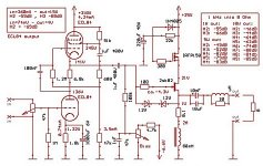
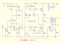
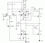
i attached some sch from designers from the different sites in the web i've search and for your comments.
Attachments
- Status
- This old topic is closed. If you want to reopen this topic, contact a moderator using the "Report Post" button.
- Home
- Amplifiers
- Solid State
- What to do with this Sony V-FETS?