You have two basic errors in this paragraph alone. Firstly, 'no triode man has ever rised this problem'. REALLY? Have you ever used a high gm triode with a fixed bias? If you look into this subject, you will notice that in most if not all cases high gm triodes and pentodes will have a caveat in their datasheet, warning to use at least partial automatic bias if not saying outright that fixed bias should not be used, and this is because this IS a problem, but it's mostly hidden by these parts normally not being used in a manner where it could become visible.
Audio Tekne of a certain IMAI that produces appreciated over that expensive valve amplifiers and triode in particular, has never used to stabilize the output voltage of its amplifiers, even in phono preamplifiers.
In your opinion, is there a reason behind this choice or do you think that is always missed the problem?
Not only he does not stabilize the output voltage also as he instead stabilizes the voltage of the grid. (perhaps to make you angrier?)

Again, you have an error in your argument which is really obvious. MOSFET/BJT outputs (disregarding for the moment the issue of thermal compensation) in case of a push-pull complementary topology have a CONSTANT VOLTAGE bias generator (Vbe multiplier etc) in 99.5% of all cases, and we were talking about using VFETs in outputs originally designed for other semiconductor devices.
This is an essential step to understand your misunderstanding.
You are referring to a scenario imagined only by you.
In fact, from the above, you are referring to use a Vfet into a "blameless topology" amplifier with the bias voltage stabilized by CCS.
But the amps I had designed with SIT clearly do not use this configuration, but are either or full symmetrical or full complementary.
However important I not use stabilizers for the gate voltage but lead track of the undulations of the mains voltage.
In truth only through an amp with 2SK180 I was forced to use a form of stabilization and here you give me a way to explain why:
By testing these devices they have shown a Vgs voltage for 100 mA between 1.5 and 3 volts only.
Now by the datasheet it were found to have a maximum current of 20 A, and this means that between 1.5 and 0 volts the current varies precisely than 20 A, so variations of Vgs of a few hundredths of a volt vary the current of several amperes and send in smoke devices (100V Vds about).
However, you know that the real stabilizers circuits are never perfect, so .......................
The basic mistake that you have committed is as follows: you have compared the behavior of Vfet Vs. the mosfet / bjt requiring the stabilization of the bias voltage and leaving the floating output voltage and then from what you have derived the result that the mosfets / bjt are more stable than Vfet.
But your reasoning is vitiated by this not necessary assumption.
Following this advice is that you care even stabilization of the output voltage, but this is a way that usually has serious consequences on the sound.
I continue to reiterate that in a simple and common bias in my opinion the Vfet are more stable per se than other solid state devices
So, if you look at various VFET designs (not the original Yamaha, Sony, Hitachi, JVC, Sansui), have a look at how bias is derived. Does it track the main power supply in the first place, let alone account for VFET mu?
Do you not think that they have taken the advantage of the phenomenon that I described in post 10?
It is a different way to say the same things.
Your observation is a clear confirmation that they are "naturally more stable" of other devices.
Best regards, Francesco
Audio Tekne of a certain IMAI that produces appreciated over that expensive valve amplifiers and triode in particular, has never used to stabilize the output voltage of its amplifiers, even in phono preamplifiers.
Honestly, this is becoming a discussion which connects the useless with uncomfortable.
Firstly, are we here talking about building a phono preamplifier with a VFET? I think not, therefore, why even mention this in comparison?
Just as an aside, I have seen just about the biggest blunders in so called 'high end' equipment, so if the designer does not understand the basic principle, does not know what consequences it has, or simply does not care, I consider it the problem of that particular designer and not mine.
The effect I have been talking about is easily demonstrable and measurable and you can hear it - now, how much of a problem it is, depends on the actual equipment and design, in particular interactions with the power supply ripple and long term stability.
Kindly refrain from quoting things like 'so and so eminence does not cater for this' in an amplifier using unspecified tubes in an unspecified configuration with unspecified power supply, because if we want to make comparisons, then we need to compare apples with apples and peanuts with peanuts and not apples with peanuts. Or, if you want to explore for yourself, try something like a SRS552/RS1003 push-pull in triode with a simple power supply (As people usually build for a simple amp) and give it a 50Hz signal, with fixed bias. NEvermind OP instability, even in such a high gm tube it's not a huge problem, but go and listen to the intermodulation. And, here we are speaking about devices with an order of magnitude higher gm, and potentially more ripple-prone supply due to high currents.
You are referring to a scenario imagined only by you.
In fact, from the above, you are referring to use a Vfet into a "blameless topology" amplifier with the bias voltage stabilized by CCS.
What I was referring to, was EXACTLY aimed at an attempt to put VFETs into something like a 'blameless' configuration, but even so most solid state designs use stabilized bias voltage (with thermal compensarion) - which is really logical since 99.99% of all designs do not use VFETs but rather pentode-characteristic semiconductors. My mentioning of this is actually directly related to Mooly's post re attempting to put VFETs into a classic topology that does not use similar semiconductors. Even Jean Hiraga fell into this trap in his conceptual drawing of the 30W class a with 2SJ20/2SK70 VFETs, and in fact introduced another problem in form of potentially fatal cross-conduction when clipping because of simply shoeing in VFETs where BJTs used to be.
But the amps I had designed with SIT clearly do not use this configuration, but are either or full symmetrical or full complementary.
This has no relevance. What I'm talking about is the way bias is derived.
However important I not use stabilizers for the gate voltage but lead track of the undulations of the mains voltage.
Hm, and where does it say so in the schematics on your website?
I do not even attempt to know what you are thinking or what you know or don't. I am only working with what you have published, which is what anyone attempting to build a VFET amp will find and perhaps try to duplicate, perhaps the person who started the thread, from whose latest question you can surmise that the issue of complementarity and phase splitting is not entirely clear. So, let's see what there is on your site:
My Sister 300 Watt SIT Super Circlotron integrated amplifier:
there are no part values nor is there any comment on tracking bias, in fact the bias is derived from a current source in the front end, multiplying the current and producing a voltage drop on fixed resistors. The current does somewhat track the front end supply voltage, but there is nothing said anywhere how this power supply is derived.
100 Watt Circlotron amplifier with Tokin SIT 2SK180:
Bias derived from a current source driven from a power supply which is in fact specifically marked as STABILIZED. Traxking? I don't think so.
50 Watt V-Fet push pull amp with 2SK70 2SJ20:
Bias is derived from the front end power supply and tracks using voltage dividers. However, no mention of the need for bias tracking. To someone who is used to the usual semiconductors, this is important to mention - in fact they might well think there is an error in the schematic because bias does track the power supply!
50 Watt V-Fet push pull amp with 2SK82 2SJ28:
Situation the same as above. BTW it would be good to mark what the source and drain terminals are on the VFETs, as these are not mutually exchangeable as on most small signal JFETs.
12 Watt single-ended with Sony V-fet 2SJ28 2SK79:
Tracking achieved by non-regulated power supply. HOWEVER - again no mention, as well as one more problem and that is lower PSRR compared to pentode character devices. OF course there will be little problems in intermodulation here if you use a CLC power supply with 10+60mF (that's mF = 1000uF), but in comparison, look at the power supplies in the previous schematics!
SIT (static induction transistor) amplifier with TKS45F323 by Kamijo:
Bias derived from power supply in a fixed way. How is the power supply derived? Is intermodulation via ripple supressed?
100 W amp with Vfet 2SK60 2SJ18:
Fixed voltage bias, not dependent on power supply at all (uses zener diodes). Of course, if you actually have the whole article where the amp is discussed, you will see it uses regulated power supplies throughout. I wonder why...
Single ended SIT amplifier with 2SK180 by Shinichi Kamijo:
Bias is mostly irelevant since it uses a VFET which is current source loaded so depends only on the current source.
V-fet amplifier 2SK60:
Bias tracks power supply. This design is derived from the Yamaha B1. It also sues positive current feedback which makes it possible to have negative output impedance! It remains a question of an in-depth analysis to see if the configuration addresses ripple compensation, but in principle it's capable of doing that. This is one of the more interesting schematics.
V-fet amplifier 2SK82:
Similar to the amp above but no mention of how the power supplies are derived, so someone attempting to duplicate it may go wrong.
Yamaha model B1 amplifier with V-fet 2SK77:
Uses regulated power supplies for everything, no mention of this...
Amplifier V-fet Sony TA 4650 with 2SJ18/2SK60:
Have a look at R324, 325, 326, 327 and R336, 337 in the driver circuit of the power amp. What could they be doing?
V-fet amplifier Hiraga with NEC 2SK70/2SJ20:
See text above. Probably never tested and drawn just as a (bad!) concept. Try this at your own peril and see what happens if you drive it to clipping.
V-fet amp Yamaha B2 with 2SK76/2SJ26:
Front end has regulated power supply. The VFET driver arrangement is quite complex and takes care of bias tracking (including ripple intermodulation supresion) and proper bias voltage sequencing on power-up. Transistors were no cheap then, they would ot have put it there if it was not needed.
Vfet amplifier Sony TAN 7B with 2SK60/2SJ18 in cascade connection:
Bias is solely defined by the bias of the BJT stages in the bottom of the cascode. It's one of the major pints of the design, the other being the creation of an extremely fast output stage.
Vfet amp Sony TAN 5550 with a pair of 2SK60/2SJ18:
Note bias generator with modulated current sources using Q501, 502, 503 - especially very small capacitor over the resistor where bias voltage is developed, to implement ripple compensation. Again, transostors were not cheap then.
V-fet amp 2SK60/2SJ18 by Furukawa:
Bias minimally tracks the +-41.5V front end power supply, as most is derived by LEDs which are essentially fixed voltage. No mention of how the front end or power stage supply should be derived or of bias tracking.
In truth only through an amp with 2SK180 I was forced to use a form of stabilization...
Which shows that the problem does exist. And still, in your posts here you have again missed the point - VFETs in general are low Gm compared to MOSFET and especially BJT, and they are thermally stable. The same problem results in bias shifting with Vds (power stage supply voltage) if bias voltage does not track, BUT unless you are using a huge VFET this is unlikely to be a major problem, except in the case where you operate the VFET very close to max specs, or in the case of PP output, lean class AB, in which case lowering the bias voltage might result in insufficient bias current to prevent crossover distortion.
However, this same problem results in intermodulation of the power supply ripple and output signal, regardless of topology (although the effect is slightly different in SE and PP), unless there is a mechanism to compensate this, or the power supply is sufficiently ripple-free so that other distortion mechanisms dominate. It is mainly this part that I am pointing out and you have not addressed it in your posts.
The other part I am pointing out, again, is that people will see what they see on your site, and coming from other semiconductors, be unaware of the problem at all - there is no discussion or warning of it, and not even of the much more problematic area of power supply sequencing. Hence my initial warning that the schematics on your site should not just be taken for granted and indeed you have already mentioned in your responses here methods of power sequencing and the problem with 2SK180 - so why is there no mention of it on the website?
The basic mistake that you have committed is as follows: you have compared the behavior of Vfet Vs. the mosfet / bjt requiring the stabilization of the bias voltage and leaving the floating output voltage and then from what you have derived the result that the mosfets / bjt are more stable than Vfet.
I have not derived that MOSFET/BJT are more stable, nor have I said so in any of my posts, not with one word. What I have said is that using VFETs in circuits where bias stabilization is designed for a device like a MOSFET or BJT will result in unstable bias for a VFET - and in fact I explained shy and how to get around it. VFETs will be completely stable if the bias is derived properly as VFETs require, and more so than MOSFETs and especially BJTs, but if you put MOSFETS or BJTs in those circuits, the bias will be unstable, potentially to the extreme of everything going up in smoke - the one exception being lateral MOSFETs, however in their case the ripple intermodulation cancelling may actually result in ripple intermodulation.
Following this advice is that you care even stabilization of the output voltage, but this is a way that usually has serious consequences on the sound.
So will using a non-regulated power supply, or using CLC filtering etc etc. Nothing new there, and in fact I did mention that simple stabilization gets best results because there is no extra problem of various stability issues in the NFB based regulators. Did I ever say using a regulated power supply is any guarantee of perfect sound? No. Will you get me to say a regulated power supply invariably sounds worse? Not a chance. I'm not into dogma, plenty of churches for that, and this is not a church (although high-end audio does sometimes resemble religion
).I continue to reiterate that in a simple and common bias in my opinion the Vfet are more stable per se than other solid state devices
DC stability is more or less assured using power supply tracking unless a truly huge VFET is used, and completely stable if a bit of correction of mu is used. The same is actually true for regulated power supply but the tracking is fixed since a regulated power supply is fixed, so mu compensation is not needed. But keep in mind we are here looking at things in terms of % - and +-10 or even 30% is not a big problem for VFETs.
However, intermodulation is still a problem if only DC tracking of bias is used. It is often not practical to filter low foltage high current supplies with CLC so there can be quite a bit of ripple especially at high output power, as well as power supply sag. In these cases AC (dynamic) bias correction works wonders, and as you can see it has been used in practically all of the original VFET amps. Unlike DC bias, here we are talking dB. The current through a VFET, like a triode, is mu times less sensitive to Vds compared to Vgs - but mu is on the order of 5-10. So, assuming you have a driving voltage of about 6Vpp (usually this will give you a bit over 1W of output into 8 ohms), any ripple on the power supply will intermodulate with this with only 1/mu supression - at most 20dB. So, the supply better be VERY well filtered. Now, the question remains, are you going to use 60000uF caps or a few resistors in the bias circuit...
Last edited:
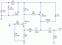
Some time ago I got some VFETs and have made a SE 5 Watt-er just to test the VFET in an amp.
Q1 is a standard JFET working at about 8mA (2SK170V can be used too). Its drain resistor (R1) provides a Vgs needed to bias a VFET (about -10V, for Id of about 1A). Working load for k60 is a 120mH choke (made by my friend, and I still wait for another one to make another channel).
V1 powers the Q1 and the V2 is a 60 Watt PS for laptop PC. The gain is set by R9/R4 ratio. The schematic can be further improved, but this simple one is quite enough to get a feel of VFETs. I made just one channel and it sounded very nice, so here it is...
Attachments
Some time ago I got some VFETs and have made a SE 5 Watt-er just to test the VFET in an amp.
Q1 is a standard JFET working at about 8mA (2SK170V can be used too). Its drain resistor (R1) provides a Vgs needed to bias a VFET (about -10V, for Id of about 1A). Working load for k60 is a 120mH choke (made by my friend, and I still wait for another one to make another channel).
V1 powers the Q1 and the V2 is a 60 Watt PS for laptop PC. The gain is set by R9/R4 ratio. The schematic can be further improved, but this simple one is quite enough to get a feel of VFETs. I made just one channel and it sounded very nice, so here it is...
Very interesting design, but has two points which can be improved.
1) Why not simply connect the load in parallel with the inductor? If it's sufficiently low DCR it will only have a very small DC component on it and you can get away without the 10mF cap. But that's only one problem - the way it's drawn (load to ground), the output cap and the 3.3mF cap from source to ground are actually connected in series - so the effective series capacitance is 2.48mF. Using the 'in paralel with inductor' trick, there would not be this effect, even if you still have to block the small DC with an output cap, and the 3.3mF cap could be far lower (it's actually only used to establish a ground reference so you can use feedback).
2) There is a slight problem with connecting the feedback like this but as the schematic is drawn, it's unfortunately the only way. The side effect is that there will be an increase in LF response (potentially quite high, in the subsonic range) if the time constant of the output caps and load is higher than the feedback cap and resitor, which happens if the load is of higher impedance than expected. As the schematic is drawn, the actual feedback point could be simply connected to the output after the output cap, with a slight correction in resistors to keep proper biassing as a small DC bias current will run through the load.
I think you may get a truly elegant design using the 'in parallel with inductor' trick and balancing the time constants of the NFB with the ground reference cap from the source of the VFET. In any case I like what you did, just keep your VFET properly cool
it's only intended for about 60W of dissipation but only if you keep the case temperature at 25 degrees C. Realistically, due to the thermal resistance of the case itself and the interface to the heatsink, 30W is about the maximum you can get with a VERY big heatsink.Easier said than done - choke's Rdc is 1.5 Ohms and Q2 has Id=1A which will set the DC offset across the speaker at 1.5V and that would be way too much (200 mA or more of DC current through 8 Ohms speaker's coil). 120mH choke is made with 1.2mm enameled copper wire and it is big - using a thicker wire is an option, but it demands a bigger core which will make the choke even bigger.......
1) Why not simply connect the load in parallel with the inductor?...
The rest of your proposals are OK and can be easily tested so that every builder can find out what suits his system (speakers) the best.
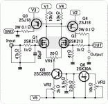
You can use the j18 in the same design. You just need to use j74V instead of BF862 and reverse the polarity of PS and capacitors. Higher power can be achieved by increasing the V2 voltage, paralleling the VFETs and raising the total current through the amp. Of course, bigger heatsinks are a must. With higher current you'll need less inductance for the same LF extension but the wire has to be thicker and the core heftier. It's all about trade-offs......how about for the J18 Pch Vfets? I had 13 Pcs of them....do you have idea where I put use on this this?...
If you want a push-pull design my choice would be a circlotron topology which, by its nature, deploys the same sex devices. If all your VFETS of the same polarity belong to the same Vgs/Id rating groups that eliminates the problem of using complementary VFETs that belong to different groups.
The choke I got from the friend was made on EI core that suits a 100VA transformer and it uses about 150 wounds of 1.2mm enameled wire to achieve 120mH at 1A....About choke any idea what the wire and core size is?
Thank you Juma...i will try to your design but i have to wind first my Chokes.
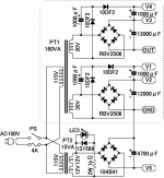
You said about circlotron....Is this circlotron from this 2SJ18 CSPP Power Amplifier
What can you comment on this?
You said about circlotron....Is this circlotron from this 2SJ18 CSPP Power Amplifier
What can you comment on this?
Attachments
"search" button is your friend:
http://www.diyaudio.com/forums/solid-state/137738-cspp-vertical-fet-2sj18.html
Anyway, that amp can sound interesting, but it lacks the basic trait of circlotron topology - absolute symmetry of the "bridge".
I'd rather go with standard circlotron idea (something like http://www.diyaudio.com/forums/pass-labs/157915-simple-cirklotron-lateral-mosfets.html ).
Of course biasing must be different - I'd use a separate circuit that would emulate battery (you can find a lot of examples of batter bias in tube world).
Shinichi Kamijo designed some SIT/VFET amplifiers and some of them are reprinted to the internet including this site.
Evolve Power Amplifiers
He explained the effect of power supply ripple on triode and equipped canceling circuit in his SIT amp.
Power Sauce Drift Cancel
He designed only one amp with complementely SEPP with J27/77 but others are circlotron.
(Circlotron is so to be called as Cross Shunt Push Pull :CSPP in Japan.)
He died last year but his website is managed his brother today.
J27/K77 SEPP design
Report
(J27! the myth do exists in the world! )
based on alexander amp topology.
His latest CSPP design
‚’ep
@ thanks Juma for the links...so its a circlotron with power PSDC...
In your simple design, V2 is 20v and V1 is 19v...is V1 a separate supply, or just the result of the dropping resistor 10 ohms R12 subtracted from V2?
I'm planning to use 48v,7A, supply which i have now and use higher voltage Jfets...what must be the IDSS rating of the Jfets required and resistor values adjustment?
Shinichi Kamijo designed some SIT/VFET amplifiers and some of them are reprinted to the internet including this site.
Evolve Power Amplifiers
He explained the effect of power supply ripple on triode and equipped canceling circuit in his SIT amp.
Power Sauce Drift Cancel
He designed only one amp with complementely SEPP with J27/77 but others are circlotron.
(Circlotron is so to be called as Cross Shunt Push Pull :CSPP in Japan.)
He died last year but his website is managed his brother today.
J27/K77 SEPP design
Report
(J27! the myth do exists in the world! )
based on alexander amp topology.
His latest CSPP design
‚’ep
Oh sad to hear that he passed away...I've been following his design in the Evolve site and they are really interesting...however some are very complex and parts are not readily available here so I can't try much..
Are there any DIYer's that tried this J18_CSPP and know how was the sound and is this design operates in class A?
what a potential!!!
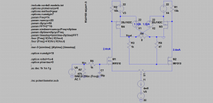
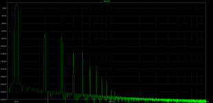
Hi
please look what great potential has this topology:
Harmonic Frequency Fourier Normalized Phase Normalized
Number [Hz] Component Component [degree] Phase [deg]
1 1.000e+03 5.464e+00 1.000e+00 -0.21° 0.00°
2 2.000e+03 5.437e-04 9.951e-05 -82.57° -82.36°
3 3.000e+03 2.502e-04 4.579e-05 26.27° 26.48°
4 4.000e+03 1.901e-06 3.480e-07 -158.70° -158.49°
5 5.000e+03 2.493e-06 4.563e-07 -134.52° -134.31°
6 6.000e+03 5.199e-08 9.515e-09 35.90° 36.11°
7 7.000e+03 3.657e-08 6.692e-09 59.92° 60.13°
8 8.000e+03 1.078e-09 1.973e-10 -135.99° -135.78°
9 9.000e+03 5.980e-10 1.095e-10 -87.74° -87.53°
Total Harmonic Distortion: 0.010954%
Thank you Juma...i will try to your design but i have to wind first my Chokes.
You said about circlotron....Is this circlotron from this 2SJ18 CSPP Power Amplifier
What can you comment on this?
Hi
please look what great potential has this topology:
Harmonic Frequency Fourier Normalized Phase Normalized
Number [Hz] Component Component [degree] Phase [deg]
1 1.000e+03 5.464e+00 1.000e+00 -0.21° 0.00°
2 2.000e+03 5.437e-04 9.951e-05 -82.57° -82.36°
3 3.000e+03 2.502e-04 4.579e-05 26.27° 26.48°
4 4.000e+03 1.901e-06 3.480e-07 -158.70° -158.49°
5 5.000e+03 2.493e-06 4.563e-07 -134.52° -134.31°
6 6.000e+03 5.199e-08 9.515e-09 35.90° 36.11°
7 7.000e+03 3.657e-08 6.692e-09 59.92° 60.13°
8 8.000e+03 1.078e-09 1.973e-10 -135.99° -135.78°
9 9.000e+03 5.980e-10 1.095e-10 -87.74° -87.53°
Total Harmonic Distortion: 0.010954%
Attachments
...In your simple design, V2 is 20v and V1 is 19v...is V1 a separate supply, ...?
Yes, it's separate PSU. I chose 20V to supply the JFET (I wanted JFET's drain at half of the V2 voltage and 10V to bias the VFET, in order to get 1A bias through it). V1 is 19V because it was convenient - it's standard value for laptop PSUs which are cheap and abundant and it suits my power and heatsink requirements. V2 needs to supply only about 10mA per channel. Each channel should have its own V1 which can be of higher voltage and/or current (depending on your speakers and power demands) but, as ilimzn said, don't go over 30W of thermal dissipation per VFET.
Shinichi Kamijo designed some SIT/VFET amplifiers and some of them are reprinted to the internet including this site.
He died last year but his website is managed his brother today.
Oh, I'm very sad to hear that. He always had very interesting topology amps.
I know, I have several
Also, there is a J25, notionally complementary to the 2SK75m used as a driver and cascode amp in the Yamaha B1.
Easier said than done - choke's Rdc is 1.5 Ohms and Q2 has Id=1A which will set the DC offset across the speaker at 1.5V and that would be way too much (200 mA or more of DC current through 8 Ohms speaker's coil). 120mH choke is made with 1.2mm enameled copper wire and it is big - using a thicker wire is an option, but it demands a bigger core which will make the choke even bigger....
The rest of your proposals are OK and can be easily tested so that every builder can find out what suits his system (speakers) the best.
Yes, if thicker wire increases choke size, then it has to be longer. At some point you get to negligible drop in DCR while the choke cost increases rapidly.
My idea was mostly to connect the load in parallel to the choke for AC (and DC if possible because it removes the cap - however, not possible in this case). So, in your schematic, the default load (1k resitor) and the load itself - the side connected to GND is moved to the 19V power supply end of the choke. This automatically removes the load current from the 3300uF cap, while all the rest stays the same. It may also be possible to transpose the load and the 10000u cap so that the connection of load and sap is at a lower DC voltage, it may be possible to establish correct DC parameters for a JFET even without the series cap in the NFB network. If not, connecting the NFB network 'after' the 10000uF cap will include it in the NFB and reduce the cap's influence on sound. However, carefull attention is needed to the value of the NFB cap and also perhaps an input cap to prevent a gain peak at LF, because the NFB will also attempt to compensate the 10000uF cap roll-off at LF, which results in a gain peak at LF and increase in distortion,
In any case it's a very interesting design. A possible variation could use an auto-former and run the VFET off a higher voltage, at lower current, so pushing the operating point into more linear regions, but as it is it's a very nice minimalistic design.
If you want a push-pull design my choice would be a circlotron topology which, by its nature, deploys the same sex devices. If all your VFETS of the same polarity belong to the same Vgs/Id rating groups that eliminates the problem of using complementary VFETs that belong to different groups.
I wholeheartedly agree! The CSPP amp schematic is a good start, with a bit of jiggling around the ground references it can have complete symmetry and still be quite simple (except for a number of power supplies - but CSPP always have that 'problem'). Again, it's also possible to use a center-tapped autoformer in such a design to get the VFETs into the more voltage, less current more linear areas, and in this case the added bonus is that the DC currents in the autoformer cancel out. Since the required inductance and ratio is low, assuming one takes care of DC balance, this could be even wound on a toroid core and offer quite high performance. Ah, so many ideas, so little time
Hi Mr. Mos57, i have some of your schematics...what do you think is the best schematic suited for my Vfets? they are not at the same rank so, can I use your complementary schematics? are those running in class A?
Thanks...
Sorry for the delay.
Not suited for complementary schematics. Mine was optimized to work in class AB but they can work also in class A, mainly bigger capacitors in PSU and heatsink only.
- Status
- This old topic is closed. If you want to reopen this topic, contact a moderator using the "Report Post" button.
- Home
- Amplifiers
- Solid State
- What to do with this Sony V-FETS?