I think that, in an LTP, (emitters of same polarity coupled) each transistor can be seen as working in the three configurations all together : EC, BC, CC. A picture of considerable help is to consider that a single transistor works as a differential device and its behaviour mainly depends on the value of the potential difference between its base and its emitter : it is voltage driven by Vbe.
The parasitic capacitances should be defined by their value and their effects described. "High" alone is not informative and comparisons are to be made with a push-pull input.
Hi forr !
My personal view is that in CFB Amp with single input BJT device ( singleton) input device work in same time in common emitter mode for input signal but in common base mode for FB signal , where sum of this two signals appear on collector .
Same operation is valid for BJT complementary input stage pair .
But maybe I`m wrong !
Best Regards !
Here are some of the things about CFA I would like to see discussed and resolved on this thread:-
4. Are comp techniques like TPC, TMC applicable to CFA (I suspect the answer to this is not straightforward)
The focus for all these questions is discrete CFA audio power amplifiers.
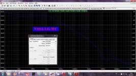
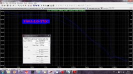
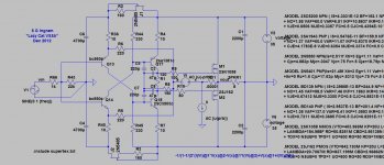
Here is VSSA simulation I did a way back in the VSSA thread. It is with MC and TMC compensation.
THD20k with MC only was 0.009388% at 30W/8ohm
THD20k with TMC was 0.002370% at 30W/8ohm
Nobody commented that at that time. Not so close to what is easily achieved with VFA but we can try to improve those figures.
Attached are LoopGain for MC and TMC, and schematic used in the simulation.
BR Damir
Attachments

Very nice one and interesting, Dadod.Here is VSSA simulation...
It seems a little early in this thread to talk about different TPC, TMC, pure Cherry compensation schemes. I hope we will have too the kgrlee participation to this passionating subject as well.
I asked Andrej and he gave the authorization to use his VSSA schematic for simulations.
I'm sure he will be very interested by those compensation studies too.
What do -you think, Dadod, because you yet have done 80% of the work, found the models etc,. to design a VFB version of this amp adding a LTP to the input stage ?
So, we can compare each aspect of the two topologies ?
Then, compensation networks studies will make this thread fantastic.
To finish by an attempt to understand better what are the characteristics related to listening experience.
Welcome in my anti acronym lobby ?Nobody commented that at that time.
http://www.acronymfinder.com/TMC.html
Last edited:
Please, refer on your data-sheets.
They do not tell the story once the components are mounted.
Hi forr !
My personal view is that in CFB Amp with single input BJT device ( singleton) input device work in same time in common emitter mode for input signal but in common base mode for FB signal , where sum of this two signals appear on collector .
Same operation is valid for BJT complementary input stage pair .
But maybe I`m wrong !
Best Regards !
Hi Banat,
I think your view is right concerning a singleton input amplifier.
Refering voltages to AC ground :
The emitter rougly replicates the voltage of the base.
The input BJT can then be seen as an emitter follower (CC).
If there is no input signal at the base, the loudspeaker acts as a microphone and delivers a signal which is submitted to the feedback network, and after attenuation, to the low impedance at the emitter. The emitter is then an input.
The input BJT can be seen as being in common base (CB).
The AC voltage difference between the base and the emitter controls the collector current which is then exploited to drive the Voltage Amplifier Stage.
The input BJT can be seen as being in common emitter (CE).
The working configuration of the input BJT is not semantically well defined except if we say it works as a combined CC-CB-CE.
This is my personal view of things, not sure everybody shares it.
Considering a BJT as a Voltage Controlled (by Vbe) Current Source (collector current) device (VCCS), albeit simplified, makes many circuits easy to understand.
forr
Excuse me if I made some gramatic mistakes since my English is pretty poor !
But must say that generally I share your views !
Actually CFB `singleton` input BJT device principle of operation remind me pretty much on principle of operation of additive RF mixing by input triode tube in RF receivers ,
where signal from antena is feed on the relative high impedance triode grid ( BJT base ),
but in the Same Time from separate oscillator unit signal is feed in to the relative low impedance triode cathode ( BJT emitter ) , sum of this two signals appear on triode anode ( BJT collector ) , later that signals sum output being further amplified , detected , ....etc .
But of course this additive signal mixing principle by Audio CFB Amps works different , since here we mix just two audio signals , one from Amp input and one from Amp output , and not just only that two audio AC signals but two DC signals to .
I think that this same principle of operation it is implemented by complementary input BJT pair by symmetric CFB Amps , for example by VSSA .
Last edited:
With a single transistor in CFA, you cannot achieve a DC coupled input and feedback in the same time, because the voltage drop in the p-n junction between the base and the emitter.by symmetric CFB Amps , for example by VSSA .
Dividing the serial resistance in two paths in a symmetrical implementation, like in the Nelson Pass F5 or the VSSA makes those DC +0.6V and -0.6V to cancel themselves across the serial feedback resistances, allowing direct coupling both for input and feedback. A simple and clever idea.
forr
Excuse me if I made some gramatic mistakes since my English is pretty poor !
But must say that generally I share your views !
Actually CFB `singleton` input BJT device principle of operation remind me pretty much on principle of operation of additive RF mixing by input triode tube in RF receivers ,
where signal from antena is feed on the relative high impedance triode grid ( BJT base ),
but in the Same Time from separate oscillator unit signal is feed in to the relative low impedance triode cathode ( BJT emitter ) , sum of this two signals appear on triode anode ( BJT collector ) , later that signals sum output being further amplified , detected , ....etc .
But of course this additive signal mixing principle by Audio CFB Amps works different , since here we mix just two audio signals , one from Amp input and one from Amp output , and not just only that two audio AC signals but two DC signals to .
I think that this same principle of operation it is implemented by complementary input BJT pair by symmetric CFB Amps , for example by VSSA .
This is very bad analogy, mixing in heterodyn receivers used unlinear behavior of triode (or hexode) to produce sum and difference frequencies and for negative feedback nonlinearity is not good thing. With NFB two very similar signals are subtracted and result is error signal.
Yes you can.Hi Esperado !
By term -DC coupled input - did you mean that audio AC signal goes straight to the BJT`s input complementary pair bases without of using of any input coupling capacitor ?
The bases are at 0V, both emitters at 0.6 and -0.6V, means the common point of the two serial feedback resistance at 0V (-0.6+0.6) that you can connect to the output of the amplifier.
Last edited:
This is very bad analogy, mixing in heterodyn receivers used unlinear behavior of triode (or hexode) to produce sum and difference frequencies and for negative feedback nonlinearity is not good thing. With NFB two very similar signals are subtracted and result is error signal.
Hi dadod !
I don`t think that this analogy is so bad at all !
Of course this `additive mixing principle`by mixing of two similar audio signals must be done in much as possible linear way using again much as possible linear SS device(s) .
Yes you can.
The bases are at 0V, both emitters at 0.6 and -0.6V, means the common point of the two serial feedback resistance at 0V (-0.6+0.6) that you can connect to the output of the amplifier.
Esperado
Thanks for your clarification !!!
Hi Guys
The most popular form of CFA uses the diamond input stage, which of course, has no voltage gain, but lots of current gain and thus power gain. With the usual overall topology for CFA, the broadband gain is on the low side, maybe 50-80db. The circuit is complimentary from input to output, and much like VFAs built this way - the Leech et al - matching of the devices becomes rather important to attain best performance.
As an example: Walt Jung had an article about a head phone amp using an opamp with a diamond buffer inside its feedback loop. His THD claims for the buffer on its own were rather dismal. This is a project anyone can build from discrete parts, and there was no attempt or suggestion to try to match anything. Besides, the huge gain of the opamp would "cure" most ills, particularly DC offsets.
Integrated diamond buffers from the early 1980s had better performance than Jung's example, but still not all that impressive by today's standards - 0.1% down to maybe 0.01% for light loading. Today, there are things like the LME49600, which boasts 0.0006% THD and can drive 250mA into a load. Not bad for a surface-mounted chip! But...
This goes to show the importance of matching whatever parts you can as well as you can.
In the MJL21193/4/5/6 data sheets, a simple EF stage is shown with matched and unmatched devices. THD drops from 0.8% to 0.08% with matching to a not-tight percentage, so something that can be screened by the manufacturer before the OEM breaks out his own test equipment.
I believe for the traditional CFA circuits, sensitivity to device matching has to be addressed, or at least recognised. ideally, we could design stages to be less sensitive to matching. You have to admit that this is one aspect of the modified Lin VFA where cost and time can be saved, but not in comp-diff inputs and push-pull VASs, nor in diamonds and comp CFAs.
I am not a fan of DC coupled amp inputs. I'd rather keep any errors from upstream out of the PA and out of the speaker. DC servos are also best avoided.
Have fun
Kevin O'Connor
Last edited:
Hi Guys
One of the error zones in the CFA is the summing node and its "non-zero" impedance. It should be relatively simple to make this a much lower impedance using either paralleled devices, or CFPs. There are also likely some asymmetric circuit options that could work well.
Have fun
Kevin O'Connor
One of the error zones in the CFA is the summing node and its "non-zero" impedance. It should be relatively simple to make this a much lower impedance using either paralleled devices, or CFPs. There are also likely some asymmetric circuit options that could work well.
Have fun
Kevin O'Connor
I am not a fan of DC coupled amp inputs. I'd rather keep any errors from upstream out of the PA and out of the speaker. DC servos are also best avoided.
Have fun
Kevin O'Connor
Hi Kevin,
Why do you say that DC servos are best avoided?
Cheers,
Bob
Priming the pump, here. The presented circuit is similar to something I built up as a first prototype on perf board back on the 1990-1991 time frame, inspired by the skeletal schematic in the AD811 data sheet at the time.
The thing actually ran and had a slew rate of ~75V/us. I never pursued it any further then, as I balked at doing the matching for the paired output fets (and yes, I had sharing issues). I'd have to scrutinize the breadboard (which still exists) to see if I parked an emitter follower between the VAS stage and the output stage. I don't think I cascoded the VAS stage back then, but I'd have to dig in and scope out the cluttered wiring to make sure. At any rate, fuel for the fire... I may revive this circuit and give it some serious class A bias, especially as I've been laying in some old TO-3 mosfets and I could possibly do some matching for the output stage (I would probably use IRF130/9130 instead of the 140/9140 shown in the schematic).
Exicon laterals might also be a possibility, simplifying the bias for the output stage.
Attachments
Hi Guys
One of the error zones in the CFA is the summing node and its "non-zero" impedance. It should be relatively simple to make this a much lower impedance using either paralleled devices, or CFPs. There are also likely some asymmetric circuit options that could work well.
Have fun
Kevin O'Connor
Hi Kevin,
By the CFP you mean Sziklai outputs? Because recently I asked gaborbela if anybody ever tried Sziklai outputs with symmetrical CFB amp (like VSSA) but there was no answer.
Hi Guys
The most popular form of CFA uses the diamond input stage, which of course, has no voltage gain, but lots of current gain and thus power gain. With the usual overall topology for CFA, the broadband gain is on the low side, maybe 50-80db. The circuit is complimentary from input to output, and much like VFAs built this way - the Leech et al - matching of the devices becomes rather important to attain best performance.
As an example: Walt Jung had an article about a head phone amp using an opamp with a diamond buffer inside its feedback loop. His THD claims for the buffer on its own were rather dismal. This is a project anyone can build from discrete parts, and there was no attempt or suggestion to try to match anything. Besides, the huge gain of the opamp would "cure" most ills, particularly DC offsets.
Integrated diamond buffers from the early 1980s had better performance than Jung's example, but still not all that impressive by today's standards - 0.1% down to maybe 0.01% for light loading. Today, there are things like the LME49600, which boasts 0.0006% THD and can drive 250mA into a load. Not bad for a surface-mounted chip! But...
This goes to show the importance of matching whatever parts you can as well as you can.
In the MJL21193/4/5/6 data sheets, a simple EF stage is shown with matched and unmatched devices. THD drops from 0.8% to 0.08% with matching to a not-tight percentage, so something that can be screened by the manufacturer before the OEM breaks out his own test equipment.
I believe for the traditional CFA circuits, sensitivity to device matching has to be addressed, or at least recognised. ideally, we could design stages to be less sensitive to matching. You have to admit that this is one aspect of the modified Lin VFA where cost and time can be saved, but not in comp-diff inputs and push-pull VASs, nor in diamonds and comp CFAs.
I am not a fan of DC coupled amp inputs. I'd rather keep any errors from upstream out of the PA and out of the speaker. DC servos are also best avoided.
Have fun
Kevin O'Connor
Good Input...... matching is extreamly important, as I pointed out in the intro on what it takes to be a CMA. Only because integrated circuit processes were developed which could make npn and pnp alike can this type circuit be competitive.
[Note - the 49600 diamond buffer has quite surprisingly high distortion. That spec is ONLY when the buffer is included within the feedback loop of a VFA. They are not well matched transistor compliments.]
THx-RNMarsh
Last edited:
Keep it Simple -
However ---> Matching of what parameters? Often there is an important one which Never gets matched by DIY'ers. Not even in SIM's of circuits. Appears to be a missed opportunity to lower distortion.
A jFET buffer and 3 resistors can be made that has THD well under .001% as I showed and explained in another forum somewhere around here. I'll throw that up over here to think about. Close matching in this case means matching the device capacitances. Look what you get when you do --- using +/-22vdc supply and a single R (3.3K) to tune the C to match and you get a null; .00008% Probably better with different devices... but to prove the point only. The highly nonlinear C's are a dominate factor.
Cascoding helps some. But not as much as this and with more cost and parts compared to a cancelling technique which can be very thorough.

Keep it simple.
THX-RNMarsh
However ---> Matching of what parameters? Often there is an important one which Never gets matched by DIY'ers. Not even in SIM's of circuits. Appears to be a missed opportunity to lower distortion.
A jFET buffer and 3 resistors can be made that has THD well under .001% as I showed and explained in another forum somewhere around here. I'll throw that up over here to think about. Close matching in this case means matching the device capacitances. Look what you get when you do --- using +/-22vdc supply and a single R (3.3K) to tune the C to match and you get a null; .00008% Probably better with different devices... but to prove the point only. The highly nonlinear C's are a dominate factor.
Cascoding helps some. But not as much as this and with more cost and parts compared to a cancelling technique which can be very thorough.
Keep it simple.
THX-RNMarsh
Last edited:
- Home
- Amplifiers
- Solid State
- CFA Topology Audio Amplifiers