Soon I'll have multiple results for the two different output stages, 2EF and standard MOS.
The only thing left to do is to try to get the most out of 2EF with the modified TPC network that yields the best result for the MOS outputs. After that I think I put them through a fair comparisson.
It's been so hot the past week that I haven't had the mojo to work on all this but things are itching")
The only thing left to do is to try to get the most out of 2EF with the modified TPC network that yields the best result for the MOS outputs. After that I think I put them through a fair comparisson.
It's been so hot the past week that I haven't had the mojo to work on all this but things are itching
The phase twists as poles are hugging up in the HF region sure can make things annoying.
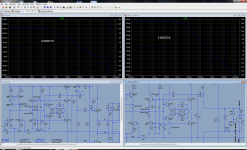
Well, I can now present 3 graphs that show a direct comparisson between the two output stages I've been focussing on. These are the standard buffered MOSFET output, and astx' 2EF BJT output.
As a starting point I took the schematic with the compensation and THD astx posted here.
The images show on the left, the MOS stage loopgain and compensation network, and on the right, the 2EF loopgain and compensation network.
With all comparisson and optimization attempts I had one simple rule: Get the phase margin at or above 60 degrees, as astx' version starts out with.
The first image shows the TMC network with values optimized for the 2EF. It shows a nice 0.000233% THD. When these values are used for the MOSFET output, you'll see that THD is much worse. However, when you look at the phase margin, it's clear these values are an over-compensation for this output stage and as such, sub optimal.
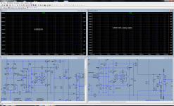
The second image shows the same TMC network, now with values optimized for the MOSFET stage. 0.000202% THD while a phase margin of 60 degrees is met. These values put in the 2EF version show a barely, if stable at all response. 60 degrees is no longer met.
This goes to show that with the same network, when optimized for the specific output stage, the THD figures are in the same ballpark.
When you compare the gain slopes, you'll see that the phase turning for the MOSFET stage sets in at a higher frequencies, with a zero showing up in the ULGF region unlike with the BJT output stage, further extending phase margin.
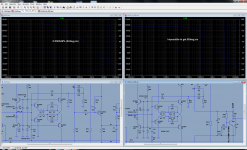
Now I went to apply the compensation I developed last, where I reverted back to the combination of Cherry with TPC, though with a T-filter instead. This compensation network is shown in the final, third picture. It pushes up available gain considerably, after setting in with a sharp decline past 100KHz. Due to less phase shift, I was able to meet a 62 degrees phase margin with this compensation. The 2EF seemingly lacking an inherent zero can't cope with this type of compensation. I tried many ranges of values, moving poles back and forth to no avail.
I think the third page shows, that at least, in this case, a higher bandwidth can be achieved with the MOS output stage. And as a result, yields better THD.
Another conclusion one can draw is that the OPS has a significant impact on the effectiveness of the compensation network used. Whether to use TMC or TPC and variants isn't always clear-cut and should be empirically figured out. But, that's probably not a surprise.
As it stands now, I'll go for the MOS output stage. Maybe more so because I still have 16 pcs of ECX10N/P20 laying about here I think this will be a nice basis for a prototype amp. I think an actual schematic and a PCB are up next
Well, I can now present 3 graphs that show a direct comparisson between the two output stages I've been focussing on. These are the standard buffered MOSFET output, and astx' 2EF BJT output.
As a starting point I took the schematic with the compensation and THD astx posted here.
The images show on the left, the MOS stage loopgain and compensation network, and on the right, the 2EF loopgain and compensation network.
With all comparisson and optimization attempts I had one simple rule: Get the phase margin at or above 60 degrees, as astx' version starts out with.
The first image shows the TMC network with values optimized for the 2EF. It shows a nice 0.000233% THD. When these values are used for the MOSFET output, you'll see that THD is much worse. However, when you look at the phase margin, it's clear these values are an over-compensation for this output stage and as such, sub optimal.
The second image shows the same TMC network, now with values optimized for the MOSFET stage. 0.000202% THD while a phase margin of 60 degrees is met. These values put in the 2EF version show a barely, if stable at all response. 60 degrees is no longer met.
This goes to show that with the same network, when optimized for the specific output stage, the THD figures are in the same ballpark.
When you compare the gain slopes, you'll see that the phase turning for the MOSFET stage sets in at a higher frequencies, with a zero showing up in the ULGF region unlike with the BJT output stage, further extending phase margin.
Now I went to apply the compensation I developed last, where I reverted back to the combination of Cherry with TPC, though with a T-filter instead. This compensation network is shown in the final, third picture. It pushes up available gain considerably, after setting in with a sharp decline past 100KHz. Due to less phase shift, I was able to meet a 62 degrees phase margin with this compensation. The 2EF seemingly lacking an inherent zero can't cope with this type of compensation. I tried many ranges of values, moving poles back and forth to no avail.
I think the third page shows, that at least, in this case, a higher bandwidth can be achieved with the MOS output stage. And as a result, yields better THD.
Another conclusion one can draw is that the OPS has a significant impact on the effectiveness of the compensation network used. Whether to use TMC or TPC and variants isn't always clear-cut and should be empirically figured out. But, that's probably not a surprise.
As it stands now, I'll go for the MOS output stage. Maybe more so because I still have 16 pcs of ECX10N/P20 laying about here
I think this will be a nice basis for a prototype amp. I think an actual schematic and a PCB are up next Attachments
Last edited:
Well, I can now present 3 graphs that show a direct comparisson between the two output stages I've been focussing on. These are the standard buffered MOSFET output, and astx' 2EF BJT output.
It would seem that you have been focusing solely on phase margin. Only one of the circuits you present has a decent gain margin.
Hi Harry;
The lower gain margin is inherent to the buffered MOS output. Only when overcompensated severely, gainmargin could be made do be 12dB+.
Still, the minimum margin is around 8dB. I thought 6dB was the minimum.
The circuit with 0.000049% THD has 8 dB margin? It looks like less than that to me?
Have you performed these loop-gain analyses at different operating points? I have already explained several times the steps you need to take to do this:
HarryDymond said:Now that you can do the loop gain plot, you can try doing it at different operating points. For example, you can try different DC operating points by AC-coupling the load with a large capacitor (e.g. 1 kF) and then adding some DC bias to the input signal. This will adjust the DC-voltage operating points of the circuit without also increasing the output current. You can also test at different current levels by adding an ideal current source from the output to ground; again, the load needs to be AC coupled.
Although I've just realised that an extra piece of advice for this would be to adjust your feedback network as necessary to make the closed-loop gain at DC equal to that at audio frequencies, assuming that currently the DC gain is unity as in most audio power amplifiers.
Are you sure that would work here? This is an inverting amplifier, DC on the input will be amplified by the total voltage gain. There's no DC blocking cap in the feedback.
OK, so your DC gain is already equal to the audio-band gain.
DC on the input will result in DC on the output. Step the DC from -x to +x, where "x" is the DC level on the input required to force the output to a level just below clipping. If you AC-couple the load (put a 1 kF capacitor in series with the load), no DC current will flow in the load due to this DC bias, but the amplifier operating points will have been adjusted to a new level.
Without DC bias, all you see is the loop-gain of the amplifier when the output signal is zero volts. What about when the amplifier is near clipping or anywhere in between? That's what the DC volts on the input will tell you.
I'm planning on starting a thread on thorough spice simulation of loop-gain. I've never tried automating the stepping process and I'm not sure how best to do it. And of course there's even more things to try, like varying the beta of BJTs etc.
I get what you're saying now. Stepping the input voltage would be easy, but trying to graph them into one overview, a trace for each step, I don't know. It's probably a tedious thing to do. Would nested stepping work?
Edit: with a bit of stretching the gain margin at cost of some THD I now ended up with 0.000097%. Still not bad.
Edit: with a bit of stretching the gain margin at cost of some THD I now ended up with 0.000097%. Still not bad.
Last edited:
Stepping the input voltage would be easy, but trying to graph them into one overview, a trace for each step, I don't know
Exactly!
I strongly recommend that you at least do a loop-gain plot for the output near clipping.
After googling I found that LTspice supports 3 nested steppings. It should then be possible to plot LG for 0*Vin , 0.1*Vin and 1*Vin (and possibly 1.1*Vin at the clipping edge). From then on it's probably copy/paste the LG function and update the run identifiers to match the Vin steps. I'll give this a try this afternoon
I think I got my final version done.. I also changed the target output specs to what I originally wanted to build:
500W/4Ohm, 250W/8Ohm
0.000093% THD @ 20KHz, full power, 8Ohm load
68deg phase margin
10.4dB gain margin
This amp, dubbed MF500 should eventually be a perfect upgrade from the old '86 Elector 1KW amp (Crescendo 1). It should have the clarity and finesse of my MF80 project, with the handsome power of a Crescendo! All thanks to fast BJT, MOSFETs and complex compensation. I already can't wait to listen to it
The outputstage PSU consists of 2x 2x55V/850VA for a total AC power of 1.7KW and an array of 8 10.000uF/100V caps, 4 per rail.
A fun detail is that one channel will amplify the inverted version of the signal, while the speaker output polarity has also been swapped to keep a net effect of zero phase. This will significantly improve OPS PSU usage as with each half wave, both the positive and negative supplies will supply current, at an about equal ratio. Both secondaries are loaded on every half wave instead of one secondary taking care of a half wave and the other of the other half wave. So both transformers are used to their full potential, on both the negative and positive half of the signal.
That should be a more than a decent supply to bring a tight, powerfull bass to life regardless of power level, up to the rated power Together with the new topology and used compensation, this should also bring a transparent, well defined sound stage at the rated power with extremely low distortion figures.
I'm soon to start on putting the OPS supply together and put it all on a base plate. Once I get to actually building the prototype, I'll open a new thread with pictures of my progress
I also changed the target output specs to what I originally wanted to build:500W/4Ohm, 250W/8Ohm
0.000093% THD @ 20KHz, full power, 8Ohm load
68deg phase margin
10.4dB gain margin
This amp, dubbed MF500 should eventually be a perfect upgrade from the old '86 Elector 1KW amp (Crescendo 1). It should have the clarity and finesse of my MF80 project, with the handsome power of a Crescendo! All thanks to fast BJT, MOSFETs and complex compensation. I already can't wait to listen to it
The outputstage PSU consists of 2x 2x55V/850VA for a total AC power of 1.7KW and an array of 8 10.000uF/100V caps, 4 per rail.
A fun detail is that one channel will amplify the inverted version of the signal, while the speaker output polarity has also been swapped to keep a net effect of zero phase. This will significantly improve OPS PSU usage as with each half wave, both the positive and negative supplies will supply current, at an about equal ratio. Both secondaries are loaded on every half wave instead of one secondary taking care of a half wave and the other of the other half wave. So both transformers are used to their full potential, on both the negative and positive half of the signal.
That should be a more than a decent supply to bring a tight, powerfull bass to life regardless of power level, up to the rated power
Together with the new topology and used compensation, this should also bring a transparent, well defined sound stage at the rated power with extremely low distortion figures.I'm soon to start on putting the OPS supply together and put it all on a base plate. Once I get to actually building the prototype, I'll open a new thread with pictures of my progress
Last edited:
Hi there,Hi,
Your power level is just about right for my use as well. The room size, speaker effeciency, and SPL all say 250W/8 minimum. Will you be offering the DIY community a way to build it... pcb etc?
Thx-RNMarsh
Yeah through the build log I would gradually add the PCBs as I design them. It's by no-means going to be an easy one to build, though I plan on keeping simple the amp design as a whole. The case is going to be 19"x40cm depth, at least, the build I'm planning. It will have a IPS/VAS supply including transformers per channel too. And I plan to use an 8-pin uC (ATtiny13) for power management, much like astx has done. It's going to be a challenge to me as every new project is. MF80 was just one step.
As for the power, yes it's great to have that an amount of power of dynamic range, especially with music that has been mastered that takes a wide dynamic range in account. At least, that's my opinion
Edit:
As for the uC's and for instance ECX10N/P20 pairs, I could assemble kits of "essential parts" once it's built and tested and distribute those.
Last edited:
Not yet, times are a bit uncertain for me. I did order two small PCBs for wiring which arrive probably in the next two weeks.
It didn't stop me from improving the simulated design though. I loosened the THD requirements some to have more flexibility for stabilization.
It's now specced 2ppm @ 20KHz/250W/8Ohm with a phasemargin of 65 degrees and a gain margin of 13dB. Still with the evil output inductor though
It didn't stop me from improving the simulated design though. I loosened the THD requirements some to have more flexibility for stabilization.
It's now specced 2ppm @ 20KHz/250W/8Ohm with a phasemargin of 65 degrees and a gain margin of 13dB. Still with the evil output inductor though
If you lose the inductor, it will be because the amplifier is creating it virtually, in which case it will be a very distorted inductor. The passive output inductor indirectly enables an amplifier to have lower distortion.
What makes it evil anyways? You can locate it away from the board by a twisted pair of wire, in any orientation you want. Even 1nF of capacitance across the inductor shouldn't matter. You could also make a toroidal air-core inductor, which just takes a little time.
What makes it evil anyways? You can locate it away from the board by a twisted pair of wire, in any orientation you want. Even 1nF of capacitance across the inductor shouldn't matter. You could also make a toroidal air-core inductor, which just takes a little time.
- Status
- This old topic is closed. If you want to reopen this topic, contact a moderator using the "Report Post" button.
- Home
- Amplifiers
- Solid State
- My New VAS Topology