Q25/26 solution!!
PanzerLord,
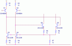
I think it is time to post my solution for the Q25/26 problem.
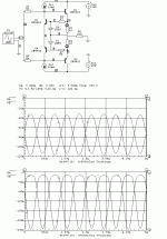
The circuit below shows it. I only added two resistors R5 and R8 and two diodes D6 and D1 (strange default labels BTW). The diodes are Infra Red LEDs of the GaAs type with a forward voltage of 1-1.2V, like CQY36. Most GaAlAs types have a higher Vf of about 1.3-1.5V and cannot be used, just as other LEDs with visible colors.
For small output currents the voltage across R3 and R4 is determined mainly by the Class A biasing and Q2 and Q4 keeps that voltage around 0.6V. The Vf of the LED is too high to have influence. If the output current is increased by a bigger input voltage or a heavier load the voltage across R3 increases for positive signals and the voltage across R4 decreases, for negative signals the other way around. Without the LEDs the maximum output current would be twice the bias current, since at that moment the voltage across R3 (or R4) becomes zero and the voltage across R4 (or R3) cannot increase beyond VbeQ2+VbeQ4. But with the LEDs the contribution of the voltage across R3 to the Q2/4 is gradually clipped, leaving some voltage left for R4. For negative signals the other way around.
This can be seen on the two graphs. The top one shows the output current through R3 and R4 with 10Vp input sine. The output stage is clearly in class A with a bias current of 70mA. The second graph shows the same but for an input signal of 30Vp. Now the stage is in class AB. But note that the current through R3 and R4 never reaches zero, just as the current through the output transistors will not go to zero. This is a "non-switching" class AB, i.e. the current is never switched off completely, nor reverse biased as you can get with normal fixed voltage biasing (Vbe multiplier).
Instead of using IR LEDs for this trick, you can also use a normal small signal Si diode and a Schottky diode in series, giving a Vf of about 1V. A third method is to use a Vbe multiplier with a multiplication factor of approx 1.6. The bigger the Vf, the smaller the minimum current will be in the output stage. If Vf becomes more than 2Vbe it will have no effect.
Of course, distortion will rise as soon the output current halves are "shaped", actually pre-distorted by the action of the LEDs. But this rise in distortion will not be so dramatic as the currents through R3 and R4 suggest. They will be subtracted from each other. The output voltage will still have a distortion less than 0.1% (open loop!). In this simulation most of the distortion comes from R1 and R9 due to varying base currents of Q1 and Q3. This will improve by using darlingtons for the ouput transistors, as in the diagram at the beginning of this thread.
The emitter resistor values are quite high in this example and only small signal transistors are used, but that is only because of my lack of models for power transistors in my free downloaded Circuitmaker program. The circuit can easily be used in power amplifiers. The value of R5 and R8 can be from 20 Ohm - 1kOhm. A small value will keep the output longer in class A without starting to shape the currents, a bigger value will increase the influence of the LEDs. This is simply because R5 and R8 are voltage dividers with the Rd of the LED as second resistor.
Steven
PS Just an idea: if you use optocouplers for the LEDs you can use the output current as an indicator whether the amplifier is in class A (no current) or class B (current). Of course these should be IR optocouplers, but I have not checked yet if these exist (or are these always IR?).
PanzerLord,
I think it is time to post my solution for the Q25/26 problem.
The circuit below shows it. I only added two resistors R5 and R8 and two diodes D6 and D1 (strange default labels BTW). The diodes are Infra Red LEDs of the GaAs type with a forward voltage of 1-1.2V, like CQY36. Most GaAlAs types have a higher Vf of about 1.3-1.5V and cannot be used, just as other LEDs with visible colors.
For small output currents the voltage across R3 and R4 is determined mainly by the Class A biasing and Q2 and Q4 keeps that voltage around 0.6V. The Vf of the LED is too high to have influence. If the output current is increased by a bigger input voltage or a heavier load the voltage across R3 increases for positive signals and the voltage across R4 decreases, for negative signals the other way around. Without the LEDs the maximum output current would be twice the bias current, since at that moment the voltage across R3 (or R4) becomes zero and the voltage across R4 (or R3) cannot increase beyond VbeQ2+VbeQ4. But with the LEDs the contribution of the voltage across R3 to the Q2/4 is gradually clipped, leaving some voltage left for R4. For negative signals the other way around.
This can be seen on the two graphs. The top one shows the output current through R3 and R4 with 10Vp input sine. The output stage is clearly in class A with a bias current of 70mA. The second graph shows the same but for an input signal of 30Vp. Now the stage is in class AB. But note that the current through R3 and R4 never reaches zero, just as the current through the output transistors will not go to zero. This is a "non-switching" class AB, i.e. the current is never switched off completely, nor reverse biased as you can get with normal fixed voltage biasing (Vbe multiplier).
Instead of using IR LEDs for this trick, you can also use a normal small signal Si diode and a Schottky diode in series, giving a Vf of about 1V. A third method is to use a Vbe multiplier with a multiplication factor of approx 1.6. The bigger the Vf, the smaller the minimum current will be in the output stage. If Vf becomes more than 2Vbe it will have no effect.
Of course, distortion will rise as soon the output current halves are "shaped", actually pre-distorted by the action of the LEDs. But this rise in distortion will not be so dramatic as the currents through R3 and R4 suggest. They will be subtracted from each other. The output voltage will still have a distortion less than 0.1% (open loop!). In this simulation most of the distortion comes from R1 and R9 due to varying base currents of Q1 and Q3. This will improve by using darlingtons for the ouput transistors, as in the diagram at the beginning of this thread.
The emitter resistor values are quite high in this example and only small signal transistors are used, but that is only because of my lack of models for power transistors in my free downloaded Circuitmaker program. The circuit can easily be used in power amplifiers. The value of R5 and R8 can be from 20 Ohm - 1kOhm. A small value will keep the output longer in class A without starting to shape the currents, a bigger value will increase the influence of the LEDs. This is simply because R5 and R8 are voltage dividers with the Rd of the LED as second resistor.
Steven
PS Just an idea: if you use optocouplers for the LEDs you can use the output current as an indicator whether the amplifier is in class A (no current) or class B (current). Of course these should be IR optocouplers, but I have not checked yet if these exist (or are these always IR?).
Attachments
As the above biasing scheme is a little off-topic for this thread and its use not limited to the amplifier that is discussed in this thread, I started a new thread for this biasing proposal here: http://www.diyaudio.com/forums/showthread.php?postid=282339#post282339
Steven
Steven
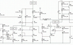
Oki, some new modifications, added a cascode in the VA stage and VA CS (ok, I cheated, I stole a bit from peufeu`s design), the cascode at the input stage has also been transformed in to a hawksford (thanks Andy C.). I`ve replaced the BD139/140 with
MJE340/350, it may become a 100W class A......, -higher rail-voltage.
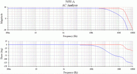
CC`s have been scrapped due to the excellent stability!! MAN, look at the bandwith and phase (without zobel-network)...
The distortion curves are almost flat throughout the audiospectrum!
I`m designing the PCB as I speak, I`m making an option for CC`s and VA without cascode, just in case the simulator`s fooling around with me).
MJE340/350, it may become a 100W class A......
, -higher rail-voltage.CC`s have been scrapped due to the excellent stability!! MAN, look at the bandwith and phase (without zobel-network)...
The distortion curves are almost flat throughout the audiospectrum!
I`m designing the PCB as I speak, I`m making an option for CC`s and VA without cascode, just in case the simulator`s fooling around with me).
Attachments
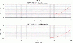
high above 10kHz? The distortion at 50kHz is less that
0.00000714% in both cases! I won`t consider that as high, I consider that extremely low...
I`ve also experimented with other bjt types, 2N3904/3906, 2SA872/2SC1775(very high beta -low noise). The design is very little dependent on bjt parameters, the only thing one has to do when replacing bjt is adjusting the current sources.
This shows that the amplifiers sound characteristic isn`t "that" dependent on the transistor type itself , but more on the actual design topology (which I belive isn`t the whole truth).
This is, however thruth when it comes to the overall distortion , no matter what bjt`s I replaced (the wilson must have equal beta bjt`s, and current sources must have high beta "reference" bjt`s), the 2nd and 3rd harmonics was below 500nV@20kHz/5uV@50kHz. That is low, (even for a pre-amp with 2V out).
In fact I measured distortion below 40mV@2MHz just now, that`s pretty wild...(this is without the zobel)
I am an advocate of high feedback through high open loop gain but I worry that your results are “too good to be true” – I am having a hard time believing the ~ 160MHz gain-bandwidth from the 50pF * 20 Ohm (20 ~=1/input stage gm) compensation time constant working with the TIP output devices
With ~4 MHz ft , the TIP output devices should limit the usable loop gain-bandwidth too much for the reported distortion to be likely, are you sure you don’t have a “disable semiconductor capacitance” switch set in your simulator software? – some simulators have this option
And I feel that the compound Baxendall super-pair VAS is wasted with the relatively low impedance from the Darlington output stage, the load on the VAS from the Darlington is ~ 100 – 300K @DC and the load should start to increase > ~20KHz (from TIP35/6 output device Hfe roll off) – with such a low VAS load a simple cascode should be fine without the potential instability we are discussing in the Baxendall thread
The two pole compensation also loads the VAS; if the compensation network isn’t driven from a low impedance such as the mje emitter or the output, the two pole cap ratio should be resized to ~ 1:1 to minimize the load impedance
I don`t use the TIP devices for anymore, the simulation is done with MJ15001/15002 (hmm, ft=2MHz...?), and the 2-pole CC is gone...
By the way, I think you got a point regarding the baxandall, I replaced it with an ordinary cascode, and it didn`t show significant changes in distortion (or bandwith)...
By the way, I think you got a point regarding the baxandall, I replaced it with an ordinary cascode, and it didn`t show significant changes in distortion (or bandwith)...

- Status
- This old topic is closed. If you want to reopen this topic, contact a moderator using the "Report Post" button.
- Home
- Amplifiers
- Solid State
- My 50W class A design!