Hello everyone, I`ve gathered a lot of useful hints and tips on this forum, so I though I`d share my project (me proud!).
I`m currently etching the PCB`s and waiting for heatsinks and output transistors to arrive, so it will probably take a couple of weeks before I can realize it in the real world. It would have been fun if someone else also has buildt this, in this way I could get some feedback on possible improvement and so on...
Okidoki, here are the facts
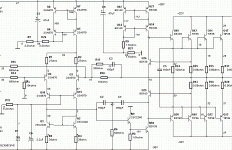
It`s a 50W class A balanced power amplifier.
-Differential input with cascode loading and current mirror
-All current sources are modified wilsons, the rolls royce of current sources
-2-pole compensation in the VA-stage(local feedback)
somewhat close to the ones I got in multisim.
-3 sets of push-pull output transistors.
-A heatsink with thermal resistance less than 0.3C/W per channel should do.
The reason I achieved these S/N, and THD levels, where the use of current sources, cascode at input , degeneration resistors, tail current tweaking (with respect to the CC), two-pole compensation, and of course the current mirror in the input stage.
The current sources and current mirror alone improves the THD+N by over 5000 times, the cascode then improves the THD by 40-50% (increased linearity).
In multisim, the simulation results where far beyond the spesifications I set as a minimum before I began designing the amplifier. (However, the results where even better when I drove the input unbalanced. The reason to this is probably differential input inbalance, I`ll look in to that in the next days).
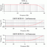
(interpolation level was set to 12, and sampling frequenzy to 128kHz for more accurate results):
THD>0.0002% (3rd. harm: 0.4uV@1kHz, 7.5uV@20kHz
2nd. harm: 1uV@1kHz, 21uV@20kHz)
All harmonic distortion simulations with 8ohm load and full voltage swing (degeneration resistors where changed to 10ohm)!!
Due to the balanced input, noise analyzis isn`t possible (S/N>115db in unbalanced mode)
Pout 8ohm=52W RMS (with 1V loss in powersupply)
DC operating point=-6mV
I`ll post my pre-amp project in a couple weeks..
Give me some feedback on this one...
")
I`m currently etching the PCB`s and waiting for heatsinks and output transistors to arrive, so it will probably take a couple of weeks before I can realize it in the real world. It would have been fun if someone else also has buildt this, in this way I could get some feedback on possible improvement and so on...
Okidoki, here are the facts
It`s a 50W class A balanced power amplifier.
-Differential input with cascode loading and current mirror
-All current sources are modified wilsons, the rolls royce of current sources
-2-pole compensation in the VA-stage(local feedback)
somewhat close to the ones I got in multisim.
-3 sets of push-pull output transistors.
-A heatsink with thermal resistance less than 0.3C/W per channel should do.
The reason I achieved these S/N, and THD levels, where the use of current sources, cascode at input , degeneration resistors, tail current tweaking (with respect to the CC), two-pole compensation, and of course the current mirror in the input stage.
The current sources and current mirror alone improves the THD+N by over 5000 times, the cascode then improves the THD by 40-50% (increased linearity).
In multisim, the simulation results where far beyond the spesifications I set as a minimum before I began designing the amplifier. (However, the results where even better when I drove the input unbalanced. The reason to this is probably differential input inbalance, I`ll look in to that in the next days).
(interpolation level was set to 12, and sampling frequenzy to 128kHz for more accurate results):
THD>0.0002% (3rd. harm: 0.4uV@1kHz, 7.5uV@20kHz
2nd. harm: 1uV@1kHz, 21uV@20kHz)
All harmonic distortion simulations with 8ohm load and full voltage swing (degeneration resistors where changed to 10ohm)!!
Due to the balanced input, noise analyzis isn`t possible (S/N>115db in unbalanced mode)
Pout 8ohm=52W RMS (with 1V loss in powersupply)
DC operating point=-6mV
I`ll post my pre-amp project in a couple weeks..
Give me some feedback on this one...
Attachments
> Give me some feedback on this one...
You asked....
Looks like current in Q19 Q20 is undefined. I don't see a bias diode.
I assume Q25 Q26 are "protection". If that is your "bias diode", I never saw that scheme and will have to think about it. For a few months.
If Q25 Q26 are bias: you have no short-protection at all. For a home-brew with $1 transistors, that's fine, but don't loan it to your clumsy friends.
If you short the output, and feed signal, Q10 will die instantly (before the output smoke).
Some preamps may not like the low input impedances.
Input impedances are not balanced for both common-mode and differential inputs (many "balanced" input designs have this flaw).
Base bias for Q15 Q16 is referenced to the supply rail. This is good for the lower mirror, bad for the input diff-pair. If I had to choose, I'd try to keep the input diff-pair at constant collector voltage, and let the mirror suffer.
Triple-zero distortion is not going to happen outside the fantasy world of the simulator. Layout coupling will introduce more distortion than the simulator can simulate. If you commit no grave grounding sins, this amp will probably be double-zero THD through 1KHz.
The signal current variation in Q10 is quite large due to high load current and only 2 stage buffer. Many amps work fine this way, but if you are playing the numbers game you might consider either higher standing current in Q10 or a triple buffer.
As a practical matter: do you really want driver stage power supplies higher than output stage supply? It adds another power supply problem and cost. Generally cheaper to run both on the same supply rails and accept a little waste. Also it may be possible to forward-bias the C-B junctions of Q19 Q20 and blow them.
Hi,
I like it very much, very spectacular , lots of features and proffesional looking... I only have some doubts about the CCS.. I'm not used to this arangement.. Seems like the Iq is refferenced to the Vsupply.. what if there's some 100Hz humm.. Seems like that humm will 'only' be attenuated by about 40dB .. but I could be wrong.. .. have been before
Succes!!,
Thijs
I like it very much, very spectacular
, lots of features and proffesional looking... I only have some doubts about the CCS.. I'm not used to this arangement.. Seems like the Iq is refferenced to the Vsupply.. what if there's some 100Hz humm.. Seems like that humm will 'only' be attenuated by about 40dB .. but I could be wrong.. .. have been before Succes!!,
Thijs
R11, C6 D1 connected wrong? Constant voltage ACROSS emitter-collector of Q3 and Q4.
R11 to -35 V and C6, D1 to ground. You could also do a little overkill in adding a NPN instead of ground and then connect base between the emitters of Q3, Q4 (via two resitors) and C6 and D1 to it's emitter. Then you really will create constant voltage across Q3 and Q4. The collector of this NPN is connected to +35 V or something lower.
Why don't you build your VAS stage with small signal transistors and then add an extra emitter follower?
Cascode load.R11, C6 D1 connected wrong? Constant voltage ACROSS emitter-collector of Q3 and Q4.
I like it very much, very spectacular , lots of features and proffesional looking... I only have some doubts about the CCS.. I'm not used to this arangement.. Seems like the Iq is refferenced to the Vsupply.. what if there's some 100Hz humm.. Seems like that humm will 'only' be attenuated by about 40dB .. but I could be wrong.. .. have been before
The power supply for the input stage is seaparated and will consist of a bootstrapped regulator, and, the psrr with the wilson CCS is far better that with the standard diode, just try it out in your school lab!
Looks like current in Q19 Q20 is undefined. I don't see a bias diode.
the emitter resistors sets the value of Vbias (the value of these must be changed to 0.91ohm->0.7volts/ca0.8 amps), if you study the curcuit loong enough, you`ll understand that this will work. This type of biasing is used in the class A amp in R. Slone "High-Power Audio Construction Manual.
If Q25 Q26 are bias: you have no short-protection at all. For a home-brew with $1 transistors, that's fine, but don't loan it to your clumsy friends.
study the schematic a bit longer, more on protection to come
s a practical matter: do you really want driver stage power supplies higher than output stage supply? It adds another power supply problem and cost. Generally cheaper to run both on the same supply rails and accept a little waste. Also it may be possible to forward-bias the C-B junctions of Q19 Q20 and blow them
See above (the trick is to build a voltage doubler at the diode
bridge, then attach a ultra low noise regulator after the doubler, better than the one used in the A75 at www.passdiy.com)
More to come (sorry about the bad english), I was in a hurry writing this....
Hi Panzerlord,
At first glance (no time for details yet) I would say it looks good. The trick with Q25 and Q26 for biasing is also used in some Yamaha pre-amps. This works only for class A output stages and I wonder what happens if your speaker impedance drops and the amplifier needs to shift into class AB operation for higher output currents. It seems to me that at that moment the output stage will get into current limiting by the bias circuit.
Steven
The current through R19 and R13 sets a voltage across Vbe on Q25 and Q26 (-> VbeQ26/R19 ), just stare at the coupling for five mins or so and you`ll get it. I`ve been lying all night thinking about.
However:
I`ve also thought about what PRR said about input impedance, and I will look into that in the next couple of hours.
I`m thinking about replacing Q26 and Q25 with a modified Vbe multiplier....This is the first time I actually design and build an amplifier, before I have buildt from other peoples schematics, so you have to be a bit paicent. I want to put most of my effort in the design before I actually build it, in that way I`ll avoid falling into traps (I hope ).
).
And I`m very grateful for your questions and for your criticism, it makes me think twice about the various soulutions regarding the topologies I`ve used, and hopefully make my design closer to perfection..(if it at works that is....)
However:
Is a good point, thanks for bringing this up Steven, I have been so exalted about my project laltely that I`ve forgotten this.This works only for class A output stages and I wonder what happens if your speaker impedance drops and the amplifier needs to shift into class AB operation for higher output currents. It seems to me that at that moment the output stage will get into current limiting by the bias circuit.
I`ve also thought about what PRR said about input impedance, and I will look into that in the next couple of hours.
I`m thinking about replacing Q26 and Q25 with a modified Vbe multiplier....This is the first time I actually design and build an amplifier, before I have buildt from other peoples schematics, so you have to be a bit paicent. I want to put most of my effort in the design before I actually build it, in that way I`ll avoid falling into traps (I hope
).And I`m very grateful for your questions and for your criticism, it makes me think twice about the various soulutions regarding the topologies I`ve used, and hopefully make my design closer to perfection..(if it at works that is....)
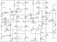
Modified input and VA stage
OK, have increased the input impedance to 10kohms
I have also replaced the current mirror with a wilson current source active load (Q1, Q2 and Q29), the results where better linearity (I had some problems with instability around 50MHz, that`s why the values of the CC`s was so high), and far better bandwith, and of course a minute improvevement in THD.
But the main task of the wilson active load is to increase the bandwith and decrease the top I had around 50MHz.
I was then allowed to lowere the values of the Two-pole CC`s to around 50pF for C2, and 300-500pF for C1, the results here where even more improvement in reducing harmonic distortion...
I have taken what Steven mentioned about lower impedance loads into considerations, and replaced the "mystic" Q25 and Q26 with a Vbe multiplier. I realised (he was right ..hehe), that, obvious, Q25 and Q26 didn`t just determine just the bias current in the output transistors, but also, on the other hand, functioned as a current limiter.
Thus, the output current was set to a total of 3 amps no matter what impedance the load had.
Once again, sorry about that bad english, guess I have to work even more on that...
OK, have increased the input impedance to 10kohms
I have also replaced the current mirror with a wilson current source active load (Q1, Q2 and Q29), the results where better linearity (I had some problems with instability around 50MHz, that`s why the values of the CC`s was so high), and far better bandwith, and of course a minute improvevement in THD.
But the main task of the wilson active load is to increase the bandwith and decrease the top I had around 50MHz.
I was then allowed to lowere the values of the Two-pole CC`s to around 50pF for C2, and 300-500pF for C1, the results here where even more improvement in reducing harmonic distortion...
I have taken what Steven mentioned about lower impedance loads into considerations, and replaced the "mystic" Q25 and Q26 with a Vbe multiplier. I realised (he was right
..hehe), that, obvious, Q25 and Q26 didn`t just determine just the bias current in the output transistors, but also, on the other hand, functioned as a current limiter.Thus, the output current was set to a total of 3 amps no matter what impedance the load had.
Once again, sorry about that bad english, guess I have to work even more on that...
Attachments

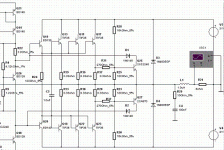
Output
Here is the new output, I`ve resized the emitter resistors, Q25 and Q27 functions as ashort circuit protection, it allows the output to deliver ca 150-200W max to the load (around 360W total, 2A max per output pair).
Have also inserted a zobel network.
The 8ohm resistor is for simulation purposes only
Attachments
or at work or in your own minilab at home, if you got one.just try it out in your school lab! quote:
I wasn`t assuming you where a student (sorry about that), I just forgot to extend the sentence, my fault, sorry!!
Maybe you are aware of this article, but for others it might be interesting: a nice tutorial about balanced inputs (and outputs). Especially input impedances are not always what you think they are, depending on how you drive the input.
http://www.dself.dsl.pipex.com/ampins/balanced/balanced.htm
Anyway, it was a good thing that you increased your input resistor at the negative input. That one was far too low in the first diagram. Even now your input is probably not 10k, as you think it is, but less. See the article above; it is described somewhere in the middle.
A nice mind-game: how can we extend the original Q25/26 construction to have its good properties for class A, while still being able to deliver more than twice the idle current if required? I have not thought about it yet, the question just pops up.
Steven
Balanced input
The way I interpretered it,it is better to have an unequal differential intput inbalance, than have an unequal CM impedance, what do you think? Is there any way I could get both equal?
I dont`t think I have enough mathematical skills to solve this problem, but thinking ALOT about ways to solve this problem.
Thanks for letting me know...
I`m stilll thinking about using the first solution using Q25 and Q26 as bias transistors...
Some of these impedances are not exactly what you would expect. In Case 3, where the input is driven as from a transformer with its centre-tap grounded, the unequal input impedances are often claimed to "unbalance the line". However, since it is common-mode interference we are trying to reject, the CM impedance is what counts, and this is the same for both inputs. The vital point is that the line output amplifier will have output impedances of 100 Ohms or less, completely dominating the line impedance. These input impedance imbalances are therefore of little significance in practice; audio connections are not transmission lines (unless they are telephone circuits several miles long) so the input impedances do not have to provide a matched and balanced termination. The low impedance of 6.7k on the cold input sounds impossible as the first thing the signal encounters is a 10k series resistor, but the crucial point is that the hot input is driven simultaneously, so the inverting op-amp input is moving in the opposite direction to the cold input, due to negative feedback, a sort of anti-bootstrapping that reduces the effective value of the 10k resistor to 6.7k. The input impedances in this mode can be made equal by manipulating resistor values, but this makes the CM impedances (to ground) unequal, which seems more undesirable.
The way I interpretered it,it is better to have an unequal differential intput inbalance, than have an unequal CM impedance, what do you think? Is there any way I could get both equal?
I dont`t think I have enough mathematical skills to solve this problem, but thinking ALOT about ways to solve this problem.
Thanks for letting me know...
I`m stilll thinking about using the first solution using Q25 and Q26 as bias transistors...
differential intput inbalance
unequal input impedance!
PanzerLord said:This is for Johanlo
Haven't really followed the thread, but two ímmediate comments
on the graphs.
1) What is the unit of magnitude in the first? dB I guess.
2) What is the level of the signal for the distorsion graphs? They
tell us nothing withoug that info.
- Status
- This old topic is closed. If you want to reopen this topic, contact a moderator using the "Report Post" button.
- Home
- Amplifiers
- Solid State
- My 50W class A design!