Hi everyone,
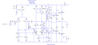
I've made this circuit, because I wanted to test the performance of a differential VAS amplifier. This topology seems to have lower distortion, and lower DC offset at the output. The major problem I've noticed with this design in particular is the lowered output excursion, caused by the Wilson Current mirrors. This design is based on one design of Bob Cordell, but it's not the same. In simulations the behaviour is very linear and has low distortions. I don't know if this amplifier with added S/C protection, DC protection and thermal shutdown could survive in the real world.
Thank you very much for your attention
Best regards,
Daniel Almeida
Attachments
I think you do not properly simulating this distortion, 0,4%-20Khz is much THD
Try this:
http://www.diyaudio.com/forums/software-tools/101810-spice-simulation-82.html#post1743578
Try this:
http://www.diyaudio.com/forums/software-tools/101810-spice-simulation-82.html#post1743578
No, that distortion seems real, which is really bad, all the amplifiers I've tried to simulate have similar or worse THD performances, including a circuit directly from Bob Cordell's website, even so this is one of the designs with less THD at 20kHz.

Best regards,
Daniel Almeida
Best regards,
Daniel Almeida
Attachments
Last edited:
Right, so you've added degeneration resistors at the LTP, and lowered the CMiller capacitor, and the result is very good, the only problem I see is the 0.1 VDC at the output, but the amplifier is really stable and has a very good phase margin, CMiller could be decreased to 68pF or 56pF and I think that the phase margin will remain acceptable.
Thank you very much,
Best regards,
Daniel Almeida
Thank you very much,
Best regards,
Daniel Almeida
I do not know the problem, got 0,023% 20KHz which is a lot for this circuit. Need to review the models Mosfets, I know little about Mosfets.
For you to loop gain, ground the input and plot the graph (right mouse - add trace) -V(Vout)/V(a) and watch your phase margin in 0 dB.
For you to loop gain, ground the input and plot the graph (right mouse - add trace) -V(Vout)/V(a) and watch your phase margin in 0 dB.
Attachments
Very interested in this topic.
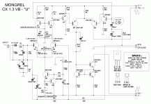
Try circuit like Mongrel CX1.3VB U, simple change output stage with SF (Source Follower). And add an active CCS for Vas.
An active CCS for Vas, maybe, not necessary. Vas's Iq controlled by Iq of Ips' CCS.
And I think Wilson Mirror for Ips too.
Pic show THD @20KHz is very low.
Try circuit like Mongrel CX1.3VB U, simple change output stage with SF (Source Follower). And add an active CCS for Vas.
An active CCS for Vas, maybe, not necessary. Vas's Iq controlled by Iq of Ips' CCS.
And I think Wilson Mirror for Ips too.
Pic show THD @20KHz is very low.
Attachments
Last edited:
Hi everyone,
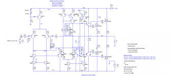
I've made this improvement using TMC (Transient Miller Compensation), with this compensation topology, the THD1 (1W-150W) is < 0.0001%, the THD20 (1W-150W) is < 0.003%.
Best regards,
Daniel Almeida
I've made this improvement using TMC (Transient Miller Compensation), with this compensation topology, the THD1 (1W-150W) is < 0.0001%, the THD20 (1W-150W) is < 0.003%.
Best regards,
Daniel Almeida
Attachments
Thank you for replying AndrewT
They are used to get a bias voltage to the differential pair of the VAS of nearly 3*vbe = 2.1 V, because at the output of the IPS/TIS the voltage is nearly 1.4V, and to prevent Q15 from entering in saturation the Vce voltage should be higher than 0.7V, in this case the Vce of Q15 is close to 1.2-1.3V to prevent the saturation. The 39k resistor allows a collector current of 1mA in transistors Q7 and Q8.
Best regards,
Daniel Almeida
- Status
- This old topic is closed. If you want to reopen this topic, contact a moderator using the "Report Post" button.
- Home
- Amplifiers
- Solid State
- Differential VAS topology