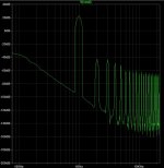
Crossover distortion visible.
This start to disappear at 14mA bias setting.
Very nice, so anywhere between 20 to 50 mA should be good to go, depending on one's wish.
Thanks for posting this.
I found some spare time to clean up the sim files.
Attached is a relabelled spice file that reflects the most recent schematic in terms of component designators. This should alleviate confusion between the sim and the schematic when refering to specific components.
This version has the output silicon that I am currently working on, so change these devices to match whatever you are using.
I am using a .step command for voltage input to find the clipping point as well as one set up for RBias to help with finding appropriate values. Set these to ;.step and reactivate the .param with your desired values once you have identified them.
----------------
Just for your viewing pleasure, I have also uploaded another version with gain set to around 25 and (I think) global feedback altered via R6. This drops the simulated THD from around 0.055 to 0.027.
This was done by reducing the 6k8 R6 to 3k6:
Gain = 1+(R6/R4) = 1+(3600/150) = 25.
Ηι avtech23,Please if isn't a big effort for you can you simulate this using R15=33R(INSTEAD OF 27R). AND bias near to zero.
I can't understand why i had measured 18v out before clip when 33R for R15 AND zero bias was used.
Last edited:
Hi Thimios, no problem:
I altered the schematic for the MJL4281 and 2sc/2sa drivers.
R15 and R8 to 33R.
R5 to 15K for symmetrical clipping.
Load to 6R
The sim shows:
450mV max input before clipping.
Output of 19.38V max output at max input across 6 ohm load.
R18 Current ~900uA
R19 Current ~130uA
R15 Current ~1.77mA
R9 Current ~1.76mA
THD 0.0758% @1KHz
This is with 'ideal' components so 19.38v ideal simulated versus ~18v real life is pretty close I think.
Attachments
Looks quite different. I may be doing something wrong. I use the Hann window when doing FFT and reduce the scale to the audible range usually. But I have played around and can't get similar results to what you have measured.
Your 13.6v, is that RMS? If it is, then 13.6*1.414 = 19.23v peak into 6 ohms which is very close to the 19.38 the simulator came up with.
Is your bias resistor (R8) set at 33R? And do you have 6.8k for R6?
Your 13.6v, is that RMS? If it is, then 13.6*1.414 = 19.23v peak into 6 ohms which is very close to the 19.38 the simulator came up with.
Is your bias resistor (R8) set at 33R? And do you have 6.8k for R6?
Looks quite different. I may be doing something wrong. I use the Hann window when doing FFT and reduce the scale to the audible range usually. But I have played around and can't get similar results to what you have measured.
Your 13.6v, is that RMS? If it is, then 13.6*1.414 = 19.23v peak into 6 ohms which is very close to the 19.38 the simulator came up with.
Is your bias resistor (R8) set at 33R? And do you have 6.8k for R6?
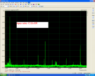
It is at 13.6V RMS/6R
No, R8 is a 220R multiturn trimmer.ADJUSTED for 10mv/0.47R.
R15=10R+15=25R.
Sim gives: 19.26v (13.62v RMS) which agrees with what you got. THD doesn't agree but there could be many reasons for that.
R8 will be in the region of 57 ohm to get 10mV (~21mA bias).
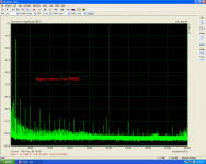
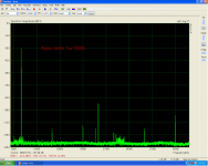
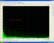
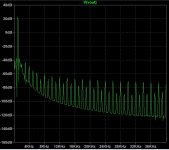
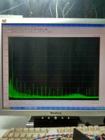
Using Kaiser7, linear Hz scale to emulate your ARTA screenshots, I get the attached FFT. I've not used the K7 before and it gives different results to the Hann or Blackman windows that I tend to use.
R8 will be in the region of 57 ohm to get 10mV (~21mA bias).
Using Kaiser7, linear Hz scale to emulate your ARTA screenshots, I get the attached FFT. I've not used the K7 before and it gives different results to the Hann or Blackman windows that I tend to use.
Attachments
ivanlukic, thank you!I found an older Mile's post at the local Serbian forum, where he gave a short explanation of AX6 circuit, and translated it. This is what he said:
AX6 has two global feedback circuits, one DC circuit before series output cap that keeps output at the half of supply voltage, and second AC feedback circuit that is taken after the output cap to lower distortion produced by the cap. VAS transistor has local feedback using emiter resistor (220R) and 100uF cap. Input transistor is compensated with 47pF to prevent ingress of ultrasonic noise at the input of amp. 27R resistor at the emiter of 2SA1837 driver helps stabilizing bias current.
You help us understanding this topology.
")
With quasi output stage, used here, you can never have ideal bias because upper driver/output pair (Darlington) requires different bias from the lower pair (Sziklai). It requires separate bias circuits for upper and lower pair. In the old times it was usual to set higher bias that suits upper pair. It's irrelevant weather you will use 10mA or 50mA because for optimum bias upper pair requires 200mA and lower 10mA.
Singleton input amps, like this one, are loved for it's specific distortion spectra. They have numerous fans.
That's why i can't see any difference even when was completely under biased.
Practically there isn't any reason for high bias-big heatsinks not for a Vbe mult.
14mA where crossover distortion disappears is fine.
Tnanks again ivanlukic!
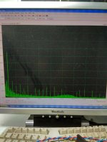
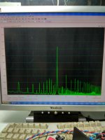
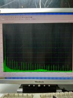
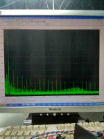
Hanning 1w RMS/6R.
Hanning 13.6v RMS/6R.
Last photo 2.8v RMS on a real 6ohm speaker.
Hanning 13.6v RMS/6R.
Last photo 2.8v RMS on a real 6ohm speaker.
Attachments
Last edited:
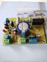
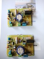
slowly but surely, only missing PS cap and o/p transistors (going to use MJL21194.)
Diodes have long legs so they can be stuck to heatsink with kapton tape like pingrs suggested.
Jumper is on btm, like thimios.
I have a 100ohm trimmer in R8' position and no R8. R5 value is 15k.
Drivers are MJE15032/33.
Other than that it follows silk more or less.
regards
Prasi
Diodes have long legs so they can be stuck to heatsink with kapton tape like pingrs suggested.
Jumper is on btm, like thimios.
I have a 100ohm trimmer in R8' position and no R8. R5 value is 15k.
Drivers are MJE15032/33.
Other than that it follows silk more or less
.regards
Prasi
Attachments
Last edited:
Prasi,well done!Bias in my board is absolutely rock stable with one diode inside a hole, just use heat shrink tube for insulation.slowly but surely, only missing PS cap and o/p transistors (going to use MJL21194.)
Diodes have long legs so they can be stuck to heatsink with kapton tape like pingrs suggested.
Jumper is on btm, like thimios.
I have a 100ohm trimmer in R8' position and no R8. R5 value is 15k.
Drivers are MJE15032/33.
Other than that it follows silk more or less
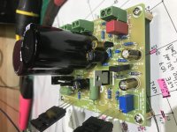
R3
regards
Prasi
R5 is the d. c feedback resistor and affect the gain. Make sure that amplifier will be stable.
Last edited:
Hi prasi,please tell us your sound impressions when using a 2.2u polypropylene cap ,you can also use a 100nF WIMA instead of the 2.2u cap to see..Thanks for your suggestions thimios, I am also planning to bypass the o/p cap with a 2.2u polypropylene cap just to see its effect.
The o/p electrolytic is a no name chinese 4700u
- Home
- Amplifiers
- Solid State
- Retro Amp 50W Single Supply