Amp design attempt number 2 (No longer simpler)
Hello all,
Decided something was fundamentally flawed with the last effort. Found the excess phase was at the non inverting input. Also, finding a satisfactory way of loading the VAS so standard miller comp could be used failed. Even though i think that amp was a failed idea I have learnt a lot.
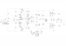
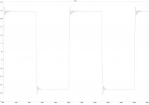
Have gone for something simpler this time. I have an obsession with the HEC at the moment, so forgive that") Cascodes were banned and I found that mixing TPC and TMC using an additional resistor works perfectly. I wish I could find where I read that trick so I could thank the person that suggested it. I was amazed at the effect it had on this amp, at least in simulation. Perfect square wave output without the need for a cap across the FB resistor.
Cascodes were banned and I found that mixing TPC and TMC using an additional resistor works perfectly. I wish I could find where I read that trick so I could thank the person that suggested it. I was amazed at the effect it had on this amp, at least in simulation. Perfect square wave output without the need for a cap across the FB resistor.
I won't bore you with THD spec's or 'owt like that. All I would like to know is whether the design looks reasonable and whether the phase plot looks ok as far as stability is concerned.
Hello all,
Decided something was fundamentally flawed with the last effort. Found the excess phase was at the non inverting input. Also, finding a satisfactory way of loading the VAS so standard miller comp could be used failed. Even though i think that amp was a failed idea I have learnt a lot.
Have gone for something simpler this time. I have an obsession with the HEC at the moment, so forgive that
Cascodes were banned and I found that mixing TPC and TMC using an additional resistor works perfectly. I wish I could find where I read that trick so I could thank the person that suggested it. I was amazed at the effect it had on this amp, at least in simulation. Perfect square wave output without the need for a cap across the FB resistor. I won't bore you with THD spec's or 'owt like that. All I would like to know is whether the design looks reasonable and whether the phase plot looks ok as far as stability is concerned.
Attachments
Last edited:
This is a current feedback type circuit, miller compensation very rarely can be used to compensate this type. Compensation should be to ground or you have your work cut out for using other compensation schemes. If you use a feedback capacitor you are sure to make it unstable, rule no1 with current feedback (youd have to change the noise gain of the circuit for it to be at least viable and that would worsen other parameters such as noise and offset).
Where is attempt no1 ??
Where is attempt no1 ??
I don't think it's a good idea to use the LTSPICE "default diode" for D5 & D6; much better to download a .MODEL of the actual diode you actually plan to use (1N914B??). I'm also concerned that C4 may be waaaay too big. See Cordell's book pp. 199-200 "The Speedup Capacitor".
Thank you for taking interest in my creations
Manso, I have found the miller compensation appears to work well in this case. I'll have to do some research on CFB amp compensation. And yes a capacitor across the feedback resistor did result in oscillation so I quickly looked for other ways to cure overshoot. Offset is something I am a little concerned about. I know its a result of the input stage and at the moment the servo is taking care of it but I wonder if there is some other way.??
mark, I have read the section you mention and understand what is being said. The counter point to that was by Rod Elliot who reckoned it was safe to make it very large. However, making it much smaller or removing it all together makes very little difference to the THD. I think I'll take it out all together. Diode choice for D5,6 is critical to THD I have found. Leakage appears adversely affect the circuit THD.
Overall feedback, here's some numbers for you
All into 8R load
20Khz THD +/-2V out = 0.000064%
20Khz THD +/-32V out = 0.001782%
1Kz THD +/- 2V out = 0.000005%
1Kz THD +/- 32V out = 0.000132%
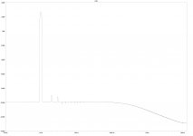
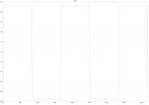
Also, here are some FFTs, square wave and clipping plots etc.
Edit: As far as I can tell the phase margin is 52 degrees with 10dB gain margin
Edit: First attempt... http://www.diyaudio.com/forums/solid-state/232662-respectable-thd-levels-double-ef-amp.html
Manso, I have found the miller compensation appears to work well in this case. I'll have to do some research on CFB amp compensation. And yes a capacitor across the feedback resistor did result in oscillation so I quickly looked for other ways to cure overshoot. Offset is something I am a little concerned about. I know its a result of the input stage and at the moment the servo is taking care of it but I wonder if there is some other way.??
mark, I have read the section you mention and understand what is being said. The counter point to that was by Rod Elliot who reckoned it was safe to make it very large. However, making it much smaller or removing it all together makes very little difference to the THD. I think I'll take it out all together. Diode choice for D5,6 is critical to THD I have found. Leakage appears adversely affect the circuit THD.
Overall feedback, here's some numbers for you
All into 8R load
20Khz THD +/-2V out = 0.000064%
20Khz THD +/-32V out = 0.001782%
1Kz THD +/- 2V out = 0.000005%
1Kz THD +/- 32V out = 0.000132%
Also, here are some FFTs, square wave and clipping plots etc.
Edit: As far as I can tell the phase margin is 52 degrees with 10dB gain margin
Edit: First attempt... http://www.diyaudio.com/forums/solid-state/232662-respectable-thd-levels-double-ef-amp.html
Attachments
Last edited:
Are you attempting to estimate gain margin and phase margin, from simulations of the closed loop amplifier? If so, that's not the right way to do it; you need to open the feedback loop and measure the gain and phase of (Vout/Vin) at the unity gain crossover frequency of the open loop amplifier ... including the gain setting voltage divider resistors (R45 and R46 of your schematic).
Please see Figure 4.7 (p.88) of Bob Cordell's book. Notice that (a) at all audio frequencies, there is no feedback; therefore the loop is open. This is because L1+C1 form a lowpass filter that filters out anything above 0.001 Hz; (b) the gain setting resistors R1 and R2 are included in the simulation; (c) the normal amplifier input port is connected to AC ground, and the test input signal is injected via Cc into the other input port for this simulation; (d) the VAS is an inverting stage, so Bob has chosen to label the IPS input pins in a way that accounts for the VAS inversion. Don't let this confuse you.
On another topic, I think I see a LOT of emitter followers + source followers in cascade (series), in your schematic. How much phase shift do each of them add, around the crossover frequency (~ 5 MHz)?
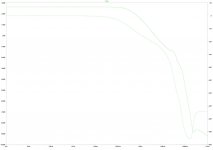
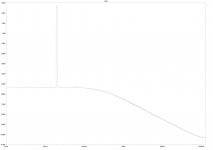
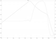
I have some strange shaped graph. It appears at 3Mhz (unity gain) the total phase at the output is +82 degrees. At the non inverting input the phase at 3MHz is +5 degrees. Most of the changes in phase happen at the ips and the vas. After Q11 not a lot changes.
How do you decipher this mass of traces into something meaningful?
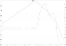
I have attached plot corresponding to where the AC meter is attached in Fig 4.7.
How do you decipher this mass of traces into something meaningful?
I have attached plot corresponding to where the AC meter is attached in Fig 4.7.
Attachments
Last edited:
I have some strange shaped graph. It appears at 3Mhz (unity gain) the total phase at the output is +82 degrees. At the non inverting input the phase at 3MHz is +5 degrees. Most of the changes in phase happen at the ips and the vas. After Q11 not a lot changes.
How do you decipher this mass of traces into something meaningful?
I have attached plot corresponding to where the AC meter is attached in Fig 4.7.
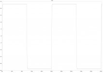
Can you make some measurements after change R40 value to about 0.3-0.1 ohm?
Yes, no problem. What would like measured?
Square and gain + phase. Plots are good the way it is, let's look for capacitive loads. I would not prefer so much driver stages for driving MOSFETs.
I know what you mean by driver stages but most are to do with implementing the HEC.
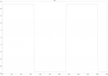
Here are plots you wanted with 0.1u set with 0.1R attached directly to V(FB). Otherwise, the LR output filter would shield the amp from the load. I figure this is a more extreme test.
Let me know if you want any more plots / measurements.
Here are plots you wanted with 0.1u set with 0.1R attached directly to V(FB). Otherwise, the LR output filter would shield the amp from the load. I figure this is a more extreme test.
Let me know if you want any more plots / measurements.
Attachments
Last edited:
I know what you mean by driver stages but most are to do with implementing the HEC.
Here are plots you wanted with 0.1u set with 0.1R attached directly to V(FB). Otherwise, the LR output filter would shield the amp from the load. I figure this is a more extreme test.
Let me know if you want any more plots / measurements.
Looks stabile like rock
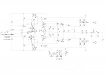
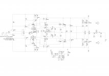
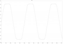
. One more plot, extreme 1uF, Square 10kHz. This is nice amp, sounds (or will sound) like this too I'm sure. I would like to look at semiconductors but text is very small. Bigger schematic will help.Thank you for the nice words about my amp. Here is the plot you wanted. I will try to post up a larger schematic for you.
It does seem very stable as long as there is 0.1R in the capacitance it is pretty much a case of choose your value.
but for now here is the plot
It does seem very stable as long as there is 0.1R in the capacitance it is pretty much a case of choose your value.
but for now here is the plot
Attachments
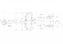
Andrew, C4 was only in place to allow for simulating the amp into capacitive loads to check for stability into extreme loads.
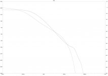
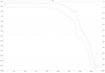
As for the 4 stage EF. I'm having problems finding a way of losing one of the last stages as the HEC configuration produces biasing voltages for higher Vgs MOSFETS. One of the EF stages is used to drop voltage. I thought of a way of dealing with this. This was to lose a stage (Q9, Q10) and change the voltage divider made up of R28, R29 and R32. This worked but square wave stability into a 1u 0.1R test load (c4) was much reduced. Maybe the base stopper resistor will need changing as well?? Had to increase C3 as well to keep stability.
I think its to do with the effective increased base stopper resistances. The 4 stage solution gave better stability into these loads and a reduced tendency to oscillate on square waves into difficult loads.
What do you think? Schematic and plot attached.
Attachments
I don't think it's a good idea to use the LTSPICE "default diode" for D5 & D6; much better to download a .MODEL of the actual diode you actually plan to use (1N914B??). I'm also concerned that C4 may be waaaay too big. See Cordell's book pp. 199-200 "The Speedup Capacitor".
Mcd99uk,
The point was that you are using bogus diode models, there. You must use a diode that can actually be purchased and installed.
So, initially at least, you have to right-click on each semiconductor that has no part number and select a real part from the list of built-in models. If you don't like any of the parts that already have models provided, then you will need to download a model for a different part.
C4 was for simulating a capacitive load directly on the MOSFET output. My understanding is that the pi network is like a shield to allow conditionally stable amplifiers to be stable by shielding the capacitive load (speakers + cables). I would like to get my amp stable so that the pi network is optional and will be included as a "belt and braces" measure.
- Status
- This old topic is closed. If you want to reopen this topic, contact a moderator using the "Report Post" button.
- Home
- Amplifiers
- Solid State
- Amp design attempt number 2 (simpler)