Hi everyone,
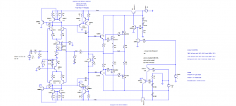
I'm simulating this circuit that is based in one circuit found in Bob Cordell's book, this circuit has good characteristics, but this is really stable in the real world, does anyone tested something like this ?
I'm thinking about using a thermal shutdown network connected to the mute network, using Schimitt Trigger configuration, and I should also use a S/C protection circuit, but I don't know if I should use a single slope VI limiter, or a multislope VI limiter.
Thank you very much for your support
Best regards,
Daniel Almeida
Attachments
I am doubtful that this circuit would work in practice. And yes, use a VI limiter; send me your email address and i'll send you an article on VI limiters. What sort of Schmitt trigger do you intend to use?
You could use the VI limiter connected to opto-coupled transistors to trigger a bistable latch that remains triggered ounce VI limiting is invoked until power is cycled.
You could use the VI limiter connected to opto-coupled transistors to trigger a bistable latch that remains triggered ounce VI limiting is invoked until power is cycled.
This circuit won't work? why?
My email adress is: danielgpsalmeida@hotmail.com
Best regards,
Daniel Almeida
My email adress is: danielgpsalmeida@hotmail.com
Best regards,
Daniel Almeida
Last edited:
Can suffer from quiescent bias current instability in the VAS, right?
Bob Cordell said that the 47kohm shunt resistor in the differential pairs should solve the problem, but I'm no sure about that, I've written in Bob Cordell's book thread.
Thank you for your help,
Best regards,
Daniel Almeida
Bob Cordell said that the 47kohm shunt resistor in the differential pairs should solve the problem, but I'm no sure about that, I've written in Bob Cordell's book thread.
Thank you for your help,
Best regards,
Daniel Almeida
Can suffer from quiescent bias current instability in the VAS, right?
Bob Cordell said that the 47kohm shunt resistor in the differential pairs should solve the problem, but I'm no sure about that....
Yes, you need to establish from Bob Cordell whether he's actually built the circuit to verify this.
Can you send me your VI limiter articles, please?
I'm thinking about using the mute network connected to a Schmitt trigger comparator, and then comparing a resistive voltage divider's voltage, with NTC voltage divider's voltage, the window will shutdown the amplifier at nearlly, I don't know, some temperature between 70 and 100 ºC and the device will only be reactivated at a lower temperature between 60 and 90 ºC, I don't know if that is possible, if so, what model of comparator I should use?
Best regards,
Daniel Almeida
Hi Guys
Yes, the idle current in the VAS is predictable and stable with the above circuit. The third Q in each mirror, Bob calls a "helper transistor'. This Q establishes the voltage on one side of the mirror. If the mirror balances, then the voltage at the output side is identical, with zero current through the 47k.
In the end, the diff tail current sets the voltage drop across the emitter Rs in the mirror. The voltage across these Rs is identical to that across the VAS emitter R, so VAS current is set by resistor ratios and the diff-amp tail current.
The same applies to the front-end of Bob's mosfet amp from 1983.
Have fun
Kevin O'Connor
Hi Guys
Yes, the idle current in the VAS is predictable and stable with the above circuit. The third Q in each mirror, Bob calls a "helper transistor'. This Q establishes the voltage on one side of the mirror. If the mirror balances, then the voltage at the output side is identical, with zero current through the 47k.
In the end, the diff tail current sets the voltage drop across the emitter Rs in the mirror. The voltage across these Rs is identical to that across the VAS emitter R, so VAS current is set by resistor ratios and the diff-amp tail current.
The same applies to the front-end of Bob's mosfet amp from 1983.
Have fun
Kevin O'Connor
Hi Kevin,
Thanks for providing this good explanation.
Stability in a circuit like this is a matter of degree and is in two aspects. First, there is the issue of VAS idle current from one amplifier to the next when no adjustment is provided for each amplifier (something one definitely does not want to do). Secondly is the temperature stability of the VAS current in a given amplifier. The matter of degree is basically referring to what one considers a reasonable tolerance due to these factors. A tolerance of +/-30% is probably acceptable for VAS standing current, but a smaller range is obviously more desirable. The bottom line is that the original Slone circuit had the VAS bias current virtually undefined, while this circuit defines it, but with tolerances.
With regard to temperature stability, if the main VAS transistor heats up and its Vbe decreases, VAS standing current will be increased. This effect is reduced in proprtion to the amount of VAS emitter degeneration. I would not recommend having less than 300mV across the VAS emitter resistor if this circuit is to be used.
Nothing comes for free. This circuit gives up some low-frequency open-loop gain in exchange for the VAS bias stability. The 47k resistor can be made a smaller value if greater stability is desired. Circuits like this are blessed with far more LF OLG than needed anyway if the output stage is a Triple.
VAS bias stability in this circuit will almost always be less than that in a single-ended current-source loaded VAS.
I should mention one more thing in connection with the current mirror "helper" transistor. I am less enamored of it than I used to be, as its use appears to cause a bit of peaking in the open-loop response when used in conjunction with a VAS preceded by an EF. AC-wise, the simple 2-transistor un-helpered VAS is better. DC-wise, for this circuit, the helper can be replaced by the same transistor diode-connected. Alternatively, one can keep the helper and bypass its base to its emitter to kill it AC-wise.
Cheers,
Bob
Hi Kevin,
I should mention one more thing in connection with the current mirror "helper" transistor. I am less enamored of it than I used to be, as its use appears to cause a bit of peaking in the open-loop response when used in conjunction with a VAS preceded by an EF. AC-wise, the simple 2-transistor un-helpered VAS is better. DC-wise, for this circuit, the helper can be replaced by the same transistor diode-connected. Alternatively, one can keep the helper and bypass its base to its emitter to kill it AC-wise.
Cheers,
Bob
Bob,
This is an interesting piece of information, as I have noticed this peaking response in simulating my attempt at designing an amp. Never even thought of looking at the current helper. I am using the jfet complementary input stage detailed in your book. My VAS is cascoded and is preceded by an EF follower.
Damn it, now I have another experiment to try in LTspice. Must have spent over 1000 hours simulating this design
")
I should mention one more thing in connection with the current mirror "helper" transistor. I am less enamored of it than I used to be, as its use appears to cause a bit of peaking in the open-loop response when used in conjunction with a VAS preceded by an EF.
Hi Bob ,
Your schematic works flawlessly assuming a single VAS transistor non enhanced is used , if enhanced a voltage shift must be created with a
diode in serial with the current mirror to increase the VAS base DC
voltage biaising.
A second point is to connect the helper transistor collector to its
commanding transistor emitter , as such the helper is inserted
in the said transistor local loop and will have limited collector current ,
as when connected like in your schematic to ground it has theoricaly
unlimited max collector current , surely the reason of the peaking.
Attachments
Hi Bob ,
Your schematic works flawlessly assuming a single VAS transistor non enhanced is used , if enhanced a voltage shift must be created with a
diode in serial with the current mirror to increase the VAS base DC
voltage biaising.
A second point is to connect the helper transistor collector to its
commanding transistor emitter , as such the helper is inserted
in the said transistor local loop and will have limited collector current ,
as when connected like in your schematic to ground it has theoricaly
unlimited max collector current , surely the reason of the peaking.
Hi wahab,
I thought I addressed your first point in my last sentence, where I mentioned inserting a diode-connected transistor in place of the helper to keep the voltages the same, or alternatively to keep the mirror helper and bypass its base-emitter to make it look like a diode at HF. Did I miss something?
I'm a little unclear on your second point, as it seems to be referring to both DC and AC aspects. Maybe it's just too early in the morning here. Maybe you could clarify by citing transistor numbers used in your schematic that you attached.
Cheers,
Bob
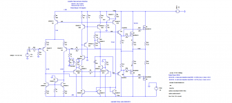
Hello Dear Mr. Bob Cordell,
and thank you very much for your help
I can't notice any peaking in the step response of the amplifier.
Is this normal, or I have some problem with my simulations?
I've to use 2*150pF capacitors, instead of two 2*30pF, because of the phase shift caused by the large gate capacitance of the used lateral MOSFET devices (BUZ901/906 by Magnatec).
I'm a newbie at discrete desgns and I don't know the methods you're telling me to use. I'm sorry, can you post some pictures, if you don't mind.
I'm still with some doubts, I don't know if it's better to make a simple current loaded VAS to start, or something more complex such as a complementary IPS-VAS topology or a differential VAS topology.
One more question, the DC current isn't limited by the 1kohm resistor and by the vbe of the current mirror transistors?
Thank you once more for your great book, and for your models and LTSpice tutorials.
Best regards,
Daniel Almeida
Attachments
Last edited:
Hi wahab,
I thought I addressed your first point in my last sentence, where I mentioned inserting a diode-connected transistor in place of the helper to keep the voltages the same, or alternatively to keep the mirror helper and bypass its base-emitter to make it look like a diode at HF. Did I miss something?
Hi Bob ,
Not sure if we are talking of the same thing here , i ll redraw the schematic
later fot this point so we can discuss it accurately.
What i m talking about is to insert diodes in serial with Q1/Q2 collectors ,
the VAS base being connected to the said transistors collectors , increasing
the voltage drop by 0.65V to make room for the enhancing transistor
VBE.
I'm a little unclear on your second point, as it seems to be referring to both DC and AC aspects. Maybe it's just too early in the morning here. Maybe you could clarify by citing transistor numbers used in your schematic that you attached.
Cheers,
Bob
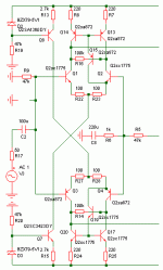
In the schematic the helpers are Q15/Q19 wich in your book have
their collectors connected to ground.
As you can see in the schematic above the helper transistors colllectors
are connected to the emitters of the relevant driving transistors.
As such , there will be no added current from ground to drive the
current mirrors , rather the driving current is taken from the current source
and localy controled by the differentials relevant transistors.
We can view Q2/Q15 and Q4/Q19 as being both CFPs arrangements, that
is , the helpers are fully part of input stage local loops.
Cheers,
wb
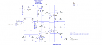
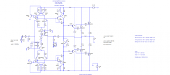
Hi everyone,
The circuits purposed by Bob Cordell attached, they worked very fine.
Thank you Bob Cordell
If you have some time, could you please read the previous post, if you don't mind?
Best regards,
Daniel Almeida
The circuits purposed by Bob Cordell attached, they worked very fine.
Thank you Bob Cordell
If you have some time, could you please read the previous post, if you don't mind?
Best regards,
Daniel Almeida
Attachments
-
 Complementary_IPS_bjt_MOSFET_output_diode_connected1.png34.1 KB · Views: 239
 -
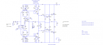 Complementary_IPS_bjt_MOSFET_output_diode_connected2.png36.8 KB · Views: 208
 -
MOSFET2_Comp_IPS_VAS_Current_Mirror_diode_connected.asc13.7 KB · Views: 37
-
MOSFET2_Comp_IPS_VAS_Current_Mirror_diode_connected2.asc13.3 KB · Views: 36
Hi Bob ,
Not sure if we are talking of the same thing here , i ll redraw the schematic
later fot this point so we can discuss it accurately.
What i m talking about is to insert diodes in serial with Q1/Q2 collectors ,
the VAS base being connected to the said transistors collectors , increasing
the voltage drop by 0.65V to make room for the enhancing transistor
VBE.
In the schematic the helpers are Q15/Q19 wich in your book have
their collectors connected to ground.
As you can see in the schematic above the helper transistors colllectors
are connected to the emitters of the relevant driving transistors.
As such , there will be no added current from ground to drive the
current mirrors , rather the driving current is taken from the current source
and localy controled by the differentials relevant transistors.
We can view Q2/Q15 and Q4/Q19 as being both CFPs arrangements, that
is , the helpers are fully part of input stage local loops.
Cheers,
wb
Hi whab, thanks for clarifying this.
To the first point, the base-emitter drop across the mirror helper elevates the DC voltage level on both sides of the current mirror so that the collectors of the two mirror transistors will now be at the same potential (2Vbe+VRE of the helpered VAS transistor). If the two collectors of the mirror were not at the same potential, current would flow through the 100k at rest, creating an undesirable offset. Vcb on both sides of the current mirror is 1Vbe.
I see what you mean about connecting the collector of the mirror helper to the emitter of, e.g., Q4. However, I usually like to flow some reasonably determined current through the helper (beyond the base current of the 2 mirror transistors) to keep its ft up. This current flowing in the emitter of Q4 would upset the balance of the diff pair. Connecting the collector of the helper to ground does not allow it to draw large currents in practice because the current of the associated mirror transistor will always increase sufficiently to cause self-limiting to occur (i.e., rise to be greater than the maximum current that Q4 can source, which is the tail current).
Cheers,
Bob
Hello Dear Mr. Bob Cordell,
and thank you very much for your help
I can't notice any peaking in the step response of the amplifier.
Is this normal, or I have some problem with my simulations?
I've to use 2*150pF capacitors, instead of two 2*30pF, because of the phase shift caused by the large gate capacitance of the used lateral MOSFET devices (BUZ901/906 by Magnatec).
I'm a newbie at discrete desgns and I don't know the methods you're telling me to use. I'm sorry, can you post some pictures, if you don't mind.
I'm still with some doubts, I don't know if it's better to make a simple current loaded VAS to start, or something more complex such as a complementary IPS-VAS topology or a differential VAS topology.
One more question, the DC current isn't limited by the 1kohm resistor and by the vbe of the current mirror transistors?
Thank you once more for your great book, and for your models and LTSpice tutorials.
Best regards,
Daniel Almeida
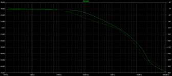
Hi Daniel,
I'm sorry I've taken so long to get to this post. It looks like you closed loop bandwidth is very small, on the order of 70kHz, if I'm interpreting your plot correctly. I'm not sure why you decided to use such large compensation capacitors with those MOSFETs. I'm not sure what value gate stoppers you used.
In general, for someone less experienced, I recommend starting with a current-loaded single-ended VAS design and really understand that first, and sharpen your skills on it. Moreover, I'd recommend starting with a BJT output stage design. The designs in Chapter 3 of my book are a good start.
BTW, in regard to current limiting, I was not clear on which 1k resistor you were referring to. Can you clarify?
Cheers,
Bob
- Status
- This old topic is closed. If you want to reopen this topic, contact a moderator using the "Report Post" button.
- Home
- Amplifiers
- Solid State
- Bob Cordell's Complementary IPS-VAS topology