SA2014 power supply reloaded ...
Final 3 pin diode variant (MBR40250TG) variant ...
IMHO: ready for fab.
Note: Schematics and Gerbers are free to use only for non commercial DIY projects.
WARNING: the circuit is using and providing very high AC and DC voltages and is therefore very dangerous and can be lethal. I am not responsible for any costs, damage and/or injury using these schematics. Do not use this schematics if you do not have the necessary experience and knowledge.
BR, Toni
Attachments
-
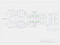 sa2014_power_supply_3pin_diodes_big_schematic.png113.5 KB · Views: 639
 -
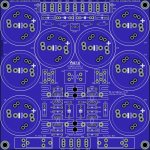 sa2014_power_supply_3pin_diodes_big_pcb_top.jpg887 KB · Views: 632
 -
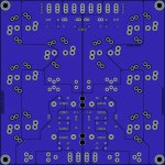 sa2014_power_supply_3pin_diodes_big_pcb_bottom.jpg456.3 KB · Views: 572
 -
sa2014_power_supply_3pin_diodes_big_schematic.pdf42.9 KB · Views: 160
-
sa2014_power_supply_3pin_diodes_big_pcb.pdf923.7 KB · Views: 156
-
sa2014_power_supply_3pin_diodes_big_pcb.zip384.8 KB · Views: 125
... clearance about 0.35mm and 1.5mm thermal.
BR, Toni
You used a clearance of 0.35mm between your copper pour zones (between nets) or is this just the thermal clearance area for a pad on that net? 0.35mm clearance between different nets seems a bit low or am I wrong?
For a power pcb's like this I usually use 0.625mm or 25mil minimum as a DRC copper clearance rule. No need to go smaller IMO.
From what I can see the clearnance for the copper fills to fills is not the same as for the fills to pads, why is that?
I can take a look at the gerber /drill data if you wish. Do you have a gerber/drill(CNC) viewer? I use mine as a sanity checker.
From what I can see the clearnance for the copper fills to fills is not the same as for the fills to pads, why is that?
I can take a look at the gerber /drill data if you wish. Do you have a gerber/drill(CNC) viewer? I use mine as a sanity checker.
"No need to go smaller" or bigger? Some online guides suggest almost 1mm for 70V. Hence my question.
In your files? "Fills to pads" on same net or another net? I've just been reviewing clearances in the version I have been playing with to learn KiCad. There one sets the properties of the copper pour plane to include clearance (overall between zones and from zone to pads etc on other nets), thermal clearance (to pads in that net) and thermal spike width. Seems to have more flex than I was aware of in Eagle. Then there is the check in DRC. (Don't look at what I sent you previously in relation to this as that was a haphazard mix of zone priority routing where clearance settings dictate gaps and more "self-driven" zone outlines.)
KiCad has a Gerber viewer.
Last edited:
Is enough for coated pcb. For DC < 100V you need 0.14mm minimum.You used a clearance of 0.35mm between your copper pour zones (between nets) or is this just the thermal clearance area for a pad on that net? 0.35mm clearance between different nets seems a bit low or am I wrong?
Uncoated you would need 0.6mm.
BR, Toni
Last edited:
This churns out 0.99mm for 80V
ANSI PCB Track Width Calculator
The author claims the formula is good for V>50
ANSI PCB Track Width Calculator
The author claims the formula is good for V>50
Those are nearer what I commonly see on our low voltage PCBs.Is enough for coated pcb. For DC < 100V you need 0.14mm minimum.
Uncoated you would need 0.6mm.
BR, Toni
Although some PCB manufacturers impose an 8thou, or 10thou, minimum for both trace widths and trace spacing.
Last edited:
yes 1mm is a better number to use for sure. The more the better.
Now that I look at the power amp rectifier pcb I did, I used 1.25mm as the fill/area spacing.
I also used copper areas instead of copper fills, so that I had full contacts instead of thermal spokes. Yes you need a hot iron with some watts behind it.
I use GerbTool as a gerber/drill(cnc) viewer. I sooner use a third party viewer than the builtin ones, as they may have the same inherent problems with interpreting the data.
WWW.CREEPAGE.COM Welcome!
Insulation: Functional
Pollution Degree: 2
Material Group: IIIa or IIIb
Working Voltage: 100 Vrms or Vdc
Coated Printed Cicuit Board? YES
Using Table 2N
Values Creepage is 0.2 mm or 7.9 mils
Wrong?
Insulation: Functional
Pollution Degree: 2
Material Group: IIIa or IIIb
Working Voltage: 100 Vrms or Vdc
Coated Printed Cicuit Board? YES
Using Table 2N
Values Creepage is 0.2 mm or 7.9 mils
Wrong?
Last edited:
Dear Steve,
indeed it's really hard to find the correct information.
Google: "en 60950-1 free download"
=> Table 2M and Table 2N
Should be save to use the power supply pcb also in Nepal in normal living room:
Altitude correction factor for levels above sea (from IEC60664-1 Table A2)
> 2000m: x 1.14
> 3000m: x 1.29
> 4000m: x 1.48
> 5000m: x 1.70
> 6000 ...
Maybe I'm completely wrong?
I have seen a few PCBs done to ~6thou/mils gaps and traces. I can see they are tiny.WWW.CREEPAGE.COM Welcome!
Insulation: Functional
Pollution Degree: 2
Material Group: IIIa or IIIb
Working Voltage: 100 Vrms or Vdc
Coated Printed Cicuit Board? YES
Using Table 2N
Values Creepage is 0.2 mm or 7.9 mils
Wrong?
Your research shows that 8thou and 10thou meet our low voltage requirements for PCBs to those conditions.
Carry on the way you have.
1mm/39.37thou/mil is monstrous as a new minimum.
That's my thinking as well - especially when we consider the use of TO-220-3 devices or devices with even more compact pins. When I looked at the calculator I found and saw circa 1mm I was rather shocked and hence the question. It does seem that regulations and guidance in this arena are very opaque. And as soon as decide to "have more where you can" zone/copper pour priority routing becomes very manual as you have to draw each pour with key rather than just using priority and a global clearance setting to automate the work for you. Probably the best thing to do is to select the maximum clearance which still gives good contact with all relevant component pins (0.5mm seems to work well enough) and manually pour for greater gap if you can be bothered.
Last edited:
Some research: The standards for audio/video are defined in EN 60065, for telecommunication and computer equipment in EN 60950 (The document numbers are mostly equal in IEC, EN, UL?!?). The newer 60065 drafts are showing harmonizing with 60950 hence the smaller distances seem to be now possible. The newest draft EN 62368-1 will replace/renew/refine the 2 standards above till 2019:
EN 62368-1 second edition successfully passed in Europe | us | TV Rheinland
So momentary it is safe using the 0.35mm clearance/creepage for a coated pcb. Will update the PCBs to 0.5mm clearance (= old 60065 for 100V) for those who are unsure (or are making the pcb's at home).
BR, Toni
BTW: the minimum distances for selfmade/uncoated PCBs are enormous - a 3 pin diode footprint will be a problem here.
Last edited:
- Home
- Amplifiers
- Solid State
- 2stageEF high performance class AB power amp / 200W8R / 400W4R