Where is the golden ratio?
To take this just a tiny bit seriously:
Hi Stee, I fail to see the golden ratio in your proposition.
"dB" is a logarithmic system (as someone pointed out) so linear mathematics aren't quite applicable.
40 dB = 10 000
24 dB = 256
ergo: 40 dB / 24 dB = 39,0625 (which incidentally is equal to 16 dB)
Yes, you see when you divide logarithmic functions you simply subtract the denominator from the numerator. Easy as pie! However, you can not divide them with each other (well, I suppose you could, but it will give you no meaningful answer)..
I don't recall either 39-something or 16 to be even close to the golden ratio..
By the way, 40/24 is EXACTLY 5/3 which (in my eyes) is a bit more elegantly written (always use primes if you can) but a VERY coarse approximation of Phi (which is the greek letter associated with the golden ratio).
An Italian guy named Leonardo Pisano Bigollo (aka "Leonardo of Pisa" or "Fibonacci") showed this back in 1202, You may have heard of him")
If I understand you correctly, you are trying to find a relation within amplifier construction that correlates to Phi. I cannot see it, so please explain how you find the golden ratio in the numbers you have provided.
If I have misunderstood something, please enlighten me.
To take this just a tiny bit seriously:
Hi Stee, I fail to see the golden ratio in your proposition.
"dB" is a logarithmic system (as someone pointed out) so linear mathematics aren't quite applicable.
40 dB = 10 000
24 dB = 256
ergo: 40 dB / 24 dB = 39,0625 (which incidentally is equal to 16 dB)
Yes, you see when you divide logarithmic functions you simply subtract the denominator from the numerator. Easy as pie! However, you can not divide them with each other (well, I suppose you could, but it will give you no meaningful answer)..
I don't recall either 39-something or 16 to be even close to the golden ratio..
By the way, 40/24 is EXACTLY 5/3 which (in my eyes) is a bit more elegantly written (always use primes if you can) but a VERY coarse approximation of Phi (which is the greek letter associated with the golden ratio).
An Italian guy named Leonardo Pisano Bigollo (aka "Leonardo of Pisa" or "Fibonacci") showed this back in 1202, You may have heard of him
If I understand you correctly, you are trying to find a relation within amplifier construction that correlates to Phi. I cannot see it, so please explain how you find the golden ratio in the numbers you have provided.
If I have misunderstood something, please enlighten me.
However, you can not divide them with each other (well, I suppose you could, but it will give you no meaningful answer)..
Exponentiation.
Really.40 dB = 10 000
24 dB = 256
Really?
It's expressing Power ratios.
As in: to make a speaker sound 40 dB louder, you need to multiply applied power by 10000X .
EDIT: so if we are analyzing the "Ratio" , it means 10000/256=39.0625 .... far from the "Golden Ratio"
And even if we were analyzing Voltage ratio, it would be 100/16=6.25 ... still very far from the classic Artistic Golden Ratio .
Which one is chosen does not matter much, anyway, as far as *none* even resembles Stee's idea.
Last edited:
Stee,
The golden ratio is based on the ratios found in the nature (like the proportions of human body), and this is the reason we find it pleasant.
Remember that an amplifier's internal construction can not be directly perceived, so adhering to the golden ratio as gain ratio does not make sense.
Of course you can make an amplifier with "golden" geometric ratios of its front panel, and it will look aesthetically pleasant...
Not to mention that (as others also pointed out) the gain is measured logarithmically, and the golden ratio is a linear relation... For example:
Zero dB amplification is an unity gain, frequently used but you can not relate it to the golden ratio.
On the other hand, you can play with the numbers as you like, and it still won't sound "golden", because there are so many other factors.
40 dB = 10 000
24 dB = 256
Really?
if he talks about power ratio it is ok, but should be
24dB - 251,2
It is a frequent confusion people asking: dB volts or dB watts? The answer is: dB is dB, but the ratio of the absolute values is different if we talk about volts or watts.
Do not write anything like "40dB in volts is 20dB in power", because this is incorrect.
I think this is a bit off-topic, but it should have been clarified.
Only if you understand such a basic term like dB will you able to come up with some new theory.
The "golden ratio" has nothing to do with dB, which is just a convenient way to express our perception that is roughly exponential.
perception of intensity
as is the case even for images
the perception of brightness occurs doubling the intensity
an aperture is twice the previous Photograph
with a simple input and one stage in simple tension
you get a gain voltage GV = 25
Normally the ratio is about 1:20 set of counterforce
place the alleged gain much more than the real one
constitutes the novelty of the golden ratio
Attachments
Stee loves symmetry, and very weird designs (that never have VALUES for their components). He reminds me of an artist who is ripping pages out of books and gluing them to a canvas, with gobs of paint and bits of hair. "Art", one might call it, but without any purpose other than to visually impress.
As an engineer, and an actual designer of circuits, I could no more attach a value-less "design" to one of these forum notes, as I could take a pile of other peoples designs, rip them up, and make "art" out of them. Its a personality thing, I guess.
But Stee is an artist. And like the majority of Art people I've met, he's way out there in the flippasphere with his theories. Magic crystals, magic ratios, magic circuit topologies that are strange, spiritually pleasing, and otherwise ... pretty kookie.
Stee... do consider restricting your "designs" to circuits that HAVE COMPONENT VALUES. Please - otherwise they're just recycled toilet paper. Anyone can draw squigs (resistors) and non-standard circuit elements, and come up with a "design". But without values, and even better, set-points (expected and real), there really is little purpose in posting the schematics as you have.
HERE IS WHY: without the circuit VALUES, none of your drawings support your idea that somehow the "golden ratio" is involved. The "ratio" is not in the circuit layout, but the components, dude. So... stop smoking the weed, get off your mushroom, and display values.
- - - - - -
Finally, on dB - although [oshifis], you're right, that you have to understand dB ... I think ti might behoove everyone to remember WHAT the definition is, in common use. We define dB as 10 log( power ratio ) ... which fits the acoustic perception picture well.
Power ratio is [power in / power out].
Since we don't have easy ways of measuring power (either "in" or "out"), but we have almost trivial ways to measure its proxy, voltage ... and since almost all circuit components respond to voltage by the formula: P = E² / Z (power = volts squared divided by impedance (which is like A/C resistance)), then using some algebra:
Pin = Ein²/Zin
Pout = Eout²/Zout
(now here's the trick: we never realize it, but in engineering, we normalize Zin to Zout!!!)
Pout/Pin = Eout²/Ein² (the z's go away, because being 'made the same', they cancel)
OK, now lets remember some logarithm identities:
log(ax) = log(a) + log(x) ... (now substitute a for x)
log(a²) = log(a) + log(a) = 2log(a)
log(a/b) = log(a) - log(b)
log(a²/b²) = log((a/b)²) = 2log(a/b) << important one
Now we just need to scale it to "our units" of the deciBel, or 10ths of a bel. Multilpy ... by 10!
10log(a²/b²) = 20log(a/b)
So there you are. dB, deciBels, remains firmly equivalenced both in the power sense, and in the normalized voltage sense.
GoatGuy
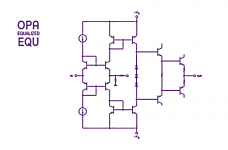
Stee,
The attached diagram is not clear.
Use the well-known formula between the closed loop gain, the open loop gain and the negative feedback.
Perhaps you could also explain what is the alleged gain.
It should be expressed in mathematical form so that we understand.
Do you afraid that someone would steal your idea, that is the reason you don't indicate component values?
Or this is just theory, and you will build the circuits after the theory will prove valid?
I also work with datasheet, pencil, paper and calculator, no simulation.
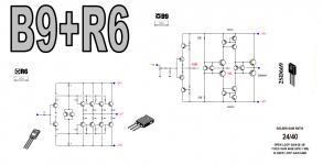
No way that 2SC2240 is passing only 2.5 mA with the (incomplete anyway) values shown, which makes me think Stee just made up some values , without thinking.
Rough reasoning, just to know where are we standing:
1) the NPN input transistor is unidentified so I am free to assume it's a 2SC2240 twin brother or very close.
2) its BE diode is in parallel with 2SC2240 BE in a current mirror configuration.
3) a current is injected: 24V/33000 ohms (not discounting the roughly 0.6V diode drop because we already have enough precision as-is)=0.72mA
4) We may safely assume it's evenly split between both parallel BE diodes, so 2SC2240 gets 0.36mA into its base.
5) datasheet shows Hfe may be anywhere between 200 and 700 , so collector current may be between 72 and 250 mA.
Although this calculation has a small error margin, and some values have spread, plus Hfe usually drops at higher current (welcome to the Real World) , the main point is that current is *WAY WAY* over what Stee made up.
His main conceptual error comes from considering a diode drop=600mV *always, no matter what* which of course is a green noob mistake.
Actual voltage drop can and does vary a lot depending on the actual part, current through it and temperature.
As a side note: that's why (despised by stee) Feedback is so important in achieving product to product repeatability.
Otherwise, you would need a dozen trimpots in every project to make things work, like in those poor "Tube to FET" conversions seen in another Forum
No way that 2SC2240 is passing only 2.5 mA with the (incomplete anyway) values shown, which makes me think Stee just made up some values , without thinking.
Rough reasoning, just to know where are we standing:
1) the NPN input transistor is unidentified
so I am free to assume it's a 2SC2240 twin brother or very close.2) its BE diode is in parallel with 2SC2240 BE in a current mirror configuration.
3) a current is injected: 24V/33000 ohms (not discounting the roughly 0.6V diode drop because we already have enough precision as-is)=0.72mA
4) We may safely assume it's evenly split between both parallel BE diodes, so 2SC2240 gets 0.36mA into its base.
5) datasheet shows Hfe may be anywhere between 200 and 700 , so collector current may be between 72 and 250 mA.
Although this calculation has a small error margin, and some values have spread, plus Hfe usually drops at higher current (welcome to the Real World) , the main point is that current is *WAY WAY* over what Stee made up.
His main conceptual error comes from considering a diode drop=600mV *always, no matter what* which of course is a green noob mistake.
Actual voltage drop can and does vary a lot depending on the actual part, current through it and temperature.
As a side note: that's why (despised by stee) Feedback is so important in achieving product to product repeatability.
Otherwise, you would need a dozen trimpots in every project to make things work, like in those poor "Tube to FET" conversions seen in another Forum
My head... is about to explode!
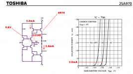
[1] Your diagram has the I/V characteristics of a 2SA970 transistor. Yet, is this the input transistor type? Not clear.
[2] You show 0.6V between C and E for the leftmost, upper transistor. Why? Remember a transistor has gain. If anything, the voltage will Iq/Hfe related. With a 33K resistor up there, at "around" 0.5 volts, with a 24 volt supply, you're talking a total of 0.7 ma. Divide by Hfe (~350) gives 2.03 uA in the base. I can't even see it on the graph, but lets say it follows the usual exponential law. 0.48V then, not 0.60V.
[3] The configuration, curiously, does NOT implement a current-mirror, although it ostensibly looks like one at the left gain stage. Instead, it is a quasi-long-tail-pair or differential mode setup. Probably with VERY high gain - essentially the Hfe of the complimentary transistor. HOWEVER, the circuit also seems to run into cut-off pretty easily. Input voltage swing can only be about 50 mV before cut-off becomes dominant.
[4] unless the 2SC2240 (circled) transistor has an Hfe about 3.5x larger than the transistor to the left, it won't be conducting 2.5 ma. Not in the least. Assuming that it is in thermal-equilibrium with its LTP mate (which is critically important for this circuit), then its current conduction at zero-input (quiescent) would be Hfe2/Hfe1 in rough terms.
[5] The negative feed-back point (input post on the 4700/47 ohm 100:1 resistive divider) actually might be better as a positive feedback: no connection leaves the emitters tied to ground via a 47R resistor. This in turn gives highest voltage gain for the LTP compliment stage. Putting positive polarity feedback on the pin reduces gain. Thus becomes "negative feedback". Whatever. its 100:1 feedback ratio.
[6] in post #48, you show the output stages. Simple emitter followers, in complimentary polarity format. Seems to me that there should be a variable resistor in series with the chain of 3 1N4148 diodes, to adjust bias of the quiescent output. Also, maybe 2 diodes would be better, as it would allow (with a variable R) more low-end control.
[7] obviously, one could chain quite a bunch of parallel-connected transistors with current-equalizing base resistors (0.47R, ea), for better output current handling. Though, I suppose at +24V to a 8 ohm load you really only have a maximum of 4 or 5 reactive amps, which a single low-voltage output transistor can handle.
[8] It is striking, and odd, that you chose the 2SA970 and 2SC2240 transistors - in that they have nominal operating points rather closer to 120 volts than 2x(24) = 48 volts. If you're going to use 100 volt transistors, at least get the supply voltage closer to the limit, as that defines a wider linear-operating region, which is especially important for transistor amplifiers.
[9] Working with a ±50V supply (still within the very-safe operating envelope of the transistors specified), AND obtaining very well matched transistor pairs, AND thermally bonding the current-mirror pairs with epoxy, AND carefully adjusting the bias points with trimmers, AND parallelizing the output transistor strip, AND carefully bonding the pre-final driver transistor to the heat-sink of the output transistors, AND adding the series-linked small-value trimpot in the diode-strip, AND hooking up the "negative-feedback" to the output line... maybe then, this would be a decent circuit. Without all those ADDs, its kind of bogus.
[10] The "problems" with it are its ultra-sensitive dependency on the Hfe ratio of the input VAS transistors, and the matching of the transistors at every current-mirror stage to at least 2 if not 3 significant digits. The incredible sensitivity of the input transistor pairs to slight thermal differences ... is just "problems waiting to happen". The output stages, being asked to deliver multiple amps to reactive loads ... have no overvoltage/back-EMF quenching diodes. Not a good design there. Also, there is no short-circuit protection... which could relatively easily be achieved if the output emitter resistors (in parallel) equal to 0.7/[max amps] ... which in turn drive the base of a pull-down complimentary pair at the pre-driver stage. Trivial, and doesn't affect sound quality as it is in cut-off in all "normal" output, except for near-short circuit conditions.
Stee...
Really old boy... this is what we're talking about. Analysis, not fuzzy-wish-thinking about great sound, with high principles, and nothing to back it up.
Oh, by the way: if it isn't clear, I don't like the circuit at all. It tries TOO hard to eliminate resistors, capacitors, and all the 'bug-bears' that have crept into the minds of "audiophiles" who have unreasonable and unfounded fetishes. A bit more straight-forward a circuit, with ... maybe boring ... but conventional VAS configurations, auto-bias-point resistor networks, very modest stage-to-stage gain, and all the above recommendations ... and you have an amplifier worth building.
GoatGuy
- Status
- This old topic is closed. If you want to reopen this topic, contact a moderator using the "Report Post" button.
- Home
- Amplifiers
- Solid State
- the Golden Gain Ratio