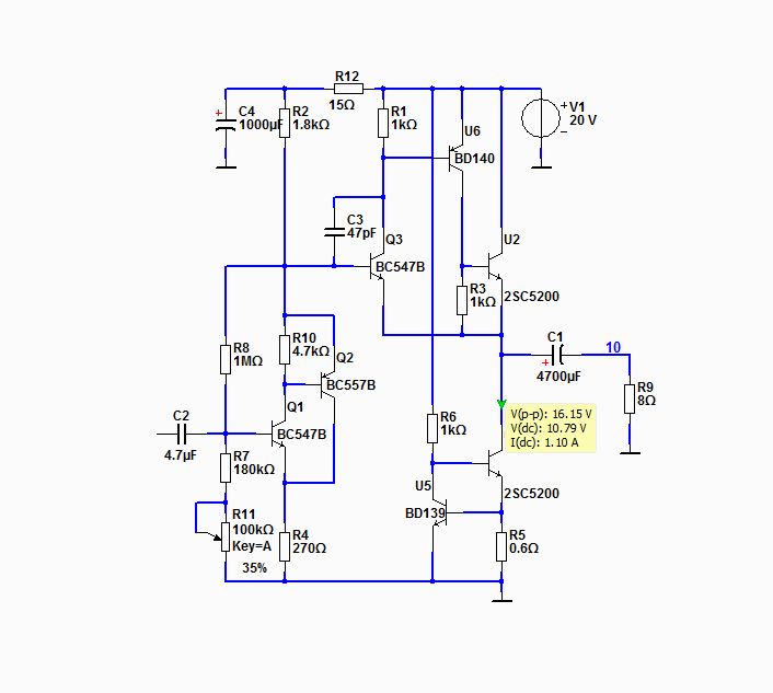
Maybe I forgot, what is the true benefit of having Q2 ?
Q2 increases the transconductance of the input stage. That means that the current through the pair of them (Q1, Q2) can swing from quite low to quite high while the VBE of Q1 changes very little. Since the voltage from the base of Q1 to its emitter vs the current through it is non-linear, this reduces the distortion of the input stage. The gain of the input stage is then almost completely determined be R2 and R4 making it a quite linear 6+2/3 or so inverting.
Hello everyone!
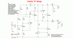
I tried the follower with TIP147 without the input circuit but with the Clepsidra preamplifier and the result is excellent.
I changed the lineup suitable scheme and simulation results me very correct and stable. Before moving to the realization I'd like to have some advice.
Thank you.
I tried the follower with TIP147 without the input circuit but with the Clepsidra preamplifier and the result is excellent.
I changed the lineup suitable scheme and simulation results me very correct and stable. Before moving to the realization I'd like to have some advice.
Thank you.
Attachments
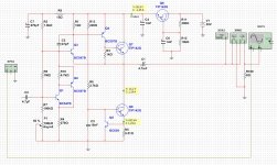
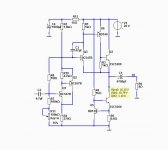
I can sense, this is a true gem!Here is the full circuit.
It delivers 4 Watt RMS into 8 Ohm with max 0.1 % distortion.
The output big transistors can be 2SC5200, MJL3281 or MJ21194.
The output DC voltage should be adjusted to V/2+0.8 Volt. Where V is the supply voltage.
Suitable transformer is 2x15 VAC. You use one winding for each channel.
One winding will give like 20-21 Volt DC supply voltage.
Enjoy")
What more could you ask for?
a mean to avoid it start oscillating with any barely capacitive load?
Last edited:
I believe he is making an assumption that it will oscillate. http://www.diyaudio.com/forums/soli...simple-circuit-great-sound-4.html#post3598199
Then is quite possible that I am doing something wrong with my LTSpice translation of the circuit, and/or, wrong sim settings...It should not oscillation. The input stage is CFP, the driver is CFP, and as long as the master device is at least twice the speed of the slave, it should be intrinsically stable, underlined by the fact it has no global feedback.
Hugh
Attachments
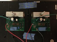
Made a board for this little guy, sounds pretty good. Excuse my ignorance, but is this inverting or non-inverting?
You could try some nch jfet instead of Q1 to hear what sounds better...
Does it oscillate with (standard test) 100nF on the output node?
You could try some nch jfet instead of Q1 to hear what sounds better...
Does it oscillate with (standard test) 100nF on the output node?
I didn't give it a torture test, I don't have a scope. Only slight change I made was using 2 x 1.2R for the lower output emitter, as I couldn't find a 0.6R in the wattage I wanted. Bias is rock soild at 1.06A and 26V rails, all seems well behaved. Version 2 will of course be with a Jfet in front.
I didn't give it a torture test, I don't have a scope. Only slight change I made was using 2 x 1.2R for the lower output emitter, as I couldn't find a 0.6R in the wattage I wanted. Bias is rock soild at 1.06A and 26V rails, all seems well behaved. Version 2 will of course be with a Jfet in front.
Ok. A lot of permutations could be tried with only few resistor value changes... due to low voltage rail, Q3 could be some jfet also.
- Home
- Amplifiers
- Solid State
- Class A, 4 Watt, No Feedback, Simple Circuit, Great Sound