A quick update. Been playing around with this design.
Changed some transistors to lower output capacitance types.
Changed the current source and attempted to cascode the VAS.
Also, changed the vbe multiplier to allow variable temp compensation.
The end result is a slight increase in high frequency distortion but can now simulate with pure capacitive loads with the output filter bypassed.
The funny thing is that the amp stability started to improve after changing to faster transistors especially the getting rid of those mje150xx drivers. Then the attempted cascode mod seemed to make things even more stable. All this goes against my belief system.
Got to say though the PCB layout is a nightmare. It has to be two layers. Its also going to have to be a two board solution with a separate PCB for the output transistors due to limited space.
Is there anything else to consider before trying to get this to work as a real circuit?
I wonder, is it even remotely sane to attempt to build this thing..?? Sane or not I'm going to have a go.
Attachments
Have a look at your Pi version of the Thiele output network.
You have 10r+C in parallel to 25r+C.
I think you could usefully make the r values much lower.
R//L maybe 2r instead of 10r
15r could maybe become 8r.
That would result in an HF load of 10r//10r for an effective 5r. Even that could still be lower and still offer good stability.
You have 10r+C in parallel to 25r+C.
I think you could usefully make the r values much lower.
R//L maybe 2r instead of 10r
15r could maybe become 8r.
That would result in an HF load of 10r//10r for an effective 5r. Even that could still be lower and still offer good stability.
Thank you for your repliues, Andrew.
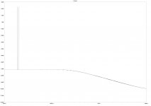
I think I have found my where the poles from the faster transistors ended up. They appear to have an effect heading up towards 80Mhz where the gain is around -80 dB.
I am I right in thinking that ideally you want your transistor poles to be as far away as possible from the dominant pole of the amplifier. Then the phase shift from the transistors will be less of a problem.
Done some experimentation with the output network. Found that the design doesn't appear to be properly stable with HF loads below 2 ohms. It doesn't oscillate but gets very distorted and their are strange currents in the drivers / predrivers.
So was thinking of using an effective HF load of 6r//6r. with 2.2r across the inductor. This appears to be stable.
Samuel Groner suggests setting R7 = R22, to get equal base currents in Q22 and Q9. Equal base currents means you're not disturbing the balance of the current mirror. Maybe you could ask the simulator to tell you Ic(Q23) and Ic(Q24) in a .OP or .DC analysis, just to see if they are well balanced. Same for R11 & R16 up top, Ic(Q25) and Ic(Q26).
The evolution continues.........
Well have been hard at work simulating and trying ideas.
Summary of changes...
1) Gone for MOSFETs of the Exicon variety. Decided that having two pairs of larger MOSFETS were the way to go. Reduce chances of parasitic oscillations. Even gives the option of only having one pair.
2) Experimented with the Hawksford error correction scheme. Found it worked well and can even be used with some changes to deal with pure capacitive loads with some penalty in distortion.
3) The Hawksford allowed smaller miller caps in the front end. But opted for a little more safety in the end.
4) Removed the separate psu circuitry for the servo. Also increased the servo output resistance. This seemed help with distortion but not really affect the offset. Having cap in place of the servo didn't work well at all.
5) Going for MOSFETs seemed to give greater output current capabilities as well as better stability. Although with a small sacrifice in power into 8 ohms but did gain 2 ohm capability.
6) All harmonics disappeared as a result of the Hawksford. Also using the 19Khz + 20Khz sine wave test resulted in two peaks in the FFT and virtually non existent harmonics.
7) Distortion levels while not amazing are good enough for me 14ppm @ 1Khz and 220ppm @ 20KHz. These can be improved but I have opted for better stability. C31 will be at least 390pF.
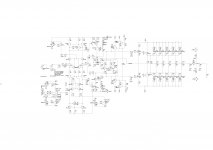
Anyway here's the circuit for anyone interested.
Bob Cordell's and Douglas Self books are superb references.
Paul
PS I know its all simulation and real life can be very different but at least I know how each component affects the results.
Well have been hard at work simulating and trying ideas.
Summary of changes...
1) Gone for MOSFETs of the Exicon variety. Decided that having two pairs of larger MOSFETS were the way to go. Reduce chances of parasitic oscillations. Even gives the option of only having one pair.
2) Experimented with the Hawksford error correction scheme. Found it worked well and can even be used with some changes to deal with pure capacitive loads with some penalty in distortion.
3) The Hawksford allowed smaller miller caps in the front end. But opted for a little more safety in the end.
4) Removed the separate psu circuitry for the servo. Also increased the servo output resistance. This seemed help with distortion but not really affect the offset. Having cap in place of the servo didn't work well at all.
5) Going for MOSFETs seemed to give greater output current capabilities as well as better stability. Although with a small sacrifice in power into 8 ohms but did gain 2 ohm capability.
6) All harmonics disappeared as a result of the Hawksford. Also using the 19Khz + 20Khz sine wave test resulted in two peaks in the FFT and virtually non existent harmonics.
7) Distortion levels while not amazing are good enough for me 14ppm @ 1Khz and 220ppm @ 20KHz. These can be improved but I have opted for better stability. C31 will be at least 390pF.
Anyway here's the circuit for anyone interested.
Bob Cordell's and Douglas Self books are superb references.
Paul
PS I know its all simulation and real life can be very different but at least I know how each component affects the results.
Attachments
Would you be kind enough to post the .asc file? I would not mind learning to sim this ckt.
Layout? What CAD pkg are you considering?
I wonder if it would be better to do this in SMT? except for the output devices, this would bring the board size down considerably. I'd give it a shot.
Layout? What CAD pkg are you considering?
I wonder if it would be better to do this in SMT? except for the output devices, this would bring the board size down considerably. I'd give it a shot.
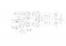
Certainly, here it is.... This the latest version, some small component value changes.
It's still under development. Need to work on the phase margin. And maybe changing to a different compensation scheme.
Will make a file of models later tonight when I have more time.
I use design spark for my PCB designs.
SMT is certainly an option. No idea of what transistors to use though.
It's still under development. Need to work on the phase margin. And maybe changing to a different compensation scheme.
Will make a file of models later tonight when I have more time.
I use design spark for my PCB designs.
SMT is certainly an option. No idea of what transistors to use though.
Attachments
I don't understand why this works....
Have been doing some playing about and experimenting with my design. I don't understand really how the compensation works but the results seem pretty reasonable.
1Khz THD = 0.000003% (+/- 33V into 8R)
20Khz THD = 0.000280% (+/- 33V into 8R)
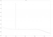
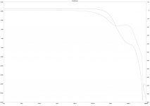
Phase margin appears to look good but the gain margin is only just ok.
I will continue tuning the circuit....
Any comments are very much appreciated. Am I going in the right direction?
Paul
Have been doing some playing about and experimenting with my design. I don't understand really how the compensation works but the results seem pretty reasonable.
1Khz THD = 0.000003% (+/- 33V into 8R)
20Khz THD = 0.000280% (+/- 33V into 8R)
Phase margin appears to look good but the gain margin is only just ok.
I will continue tuning the circuit....
Any comments are very much appreciated. Am I going in the right direction?
Paul
Attachments
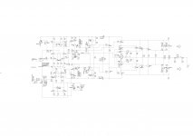
I just took a quick glance so this may be inaccurate, but I think I see a cascade of five (!) emitter followers in series:
I'd recommend you have SPICE tally up the phase contribution of each of these stages in the vicinity of the unity gain frequency. I suspect you might be getting more "excess phase" than you'd like.
- VAS ->
- Q18 ->
- Q48 ->
- Q52 ->
- Q34 ->
- U1 -> speaker
I'd recommend you have SPICE tally up the phase contribution of each of these stages in the vicinity of the unity gain frequency. I suspect you might be getting more "excess phase" than you'd like.
Yes, I agree looks like it is 5 EFs in a row. Reason for that was to try and boost the open loop gain to allow the feedback to have more head room to reduce distortion. The thinking was that MOSFETs have low gain and was trying to compensate for that. Maybe that avenue was the wrong way to go.
I will attempt to get SPICE to do as you say. More research required.
Do you remove the compensation circuitry first?
I can see two stages that could be removed. Maybe that would be worth a go and compare results.
I will attempt to get SPICE to do as you say. More research required.
Do you remove the compensation circuitry first?
I can see two stages that could be removed. Maybe that would be worth a go and compare results.
- Status
- This old topic is closed. If you want to reopen this topic, contact a moderator using the "Report Post" button.
- Home
- Amplifiers
- Solid State
- Respectable THD levels for double EF Amp