Hi fellow diy-ers. 
Update(19March2016): A couple new, improved and tested PeeCeeBee layouts have been uploaded. Links below.
Update(30December2016): PeeCeeBee V3 layout has been uploaded. The smallest yet the best sounding PeeCeeBee with 2"x2" footprint! Link below.
V1.1
Layout: >Here<
Pics:
V2
Layout: >Here<
Pics:
V3
Layout: >Here<
Pics:

(Old text from here)
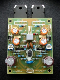
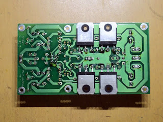
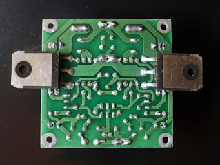
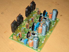
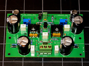
Here is the VSSA all through-hole PCB as promised. (update- we now have our first SMD PeeCeeBee! Check at the end of this post)
Dimensions: 2" x 2.7".
There is no compensation capacitors and zobel on-board. If found to be necessary then the Zobel may be connected off-board at the binding post solder joints, and the Cdom(s) under the board between B and C of the VAS trannies. These accessories may find their place in the next version of the board, can't say for sure 😉.
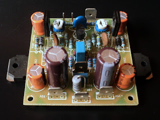
The resistors marked OFF1 and OFF2 are to be left for fine tuning of the offset. A value of between 100K and 1M at any of these will set the offset very close to zero. These should be connected after the board is fully assembled with all the other parts. Ideally any one of the two resistors will be needed. If connecting on the positive side seems to increase the offset then leave that and concentrate on the negative side only.
The amp can be run from +/-15V upto +/-35V. The only part that needs to be varied is the default 15K resistors which are for 35V operation. I Use 10K for my 16V setup. This value is best decided through direct measuring of the VAS current at the 10ohm degenerators at their emitters. 10mA is a good bias, with small "U" shaped heatsinks for the VAS. Increase to 20mA if you can keep them cold by using better heatsinks. The trannies are aligned so that a single metal piece can be used for both. Don't forget mica insulator if this is your choice.
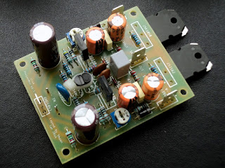
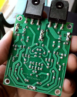
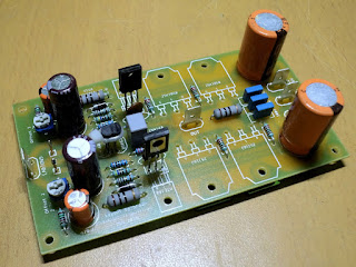
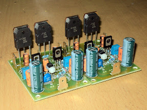
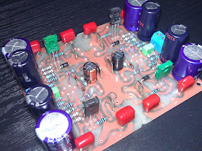
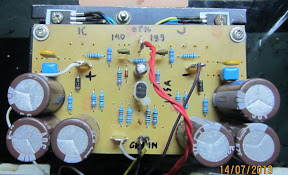
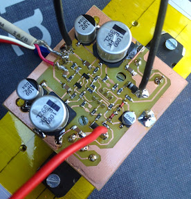
Pix of my finished and assembled boards:
If you have any queries about the board and setup etc. then feel free to post it here. I'll help as much as I can.
Happy listening.
shaan
edit:- The layout is in the VSSAbottom.pdf file.
Important:- Visitors/posters are welcome to modify any of the layouts according to their need and/or add totally new designs. However, if you want to use CCS or Multilayer Layout or Parallel capacitors in the feedback network then please post your VSSA experiment and results in the original VSSA thread. Link >Here<. This thread's topic is single layer printed circuit board designs based on the VSSA schematic without the above mentioned accessories, shown in one of the pictures attached below. Thanks for your co-operation.
Update(19/11/2014):
More Tested PeeCeeBee designs(kind contribution by fellow diy-ers):
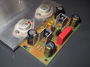
1. By PMI:- Click >Here< (Pro-style layout with under-board MOSFET mount).
2. By Jason:- Click >Here< (TO3 output MOSFETs)
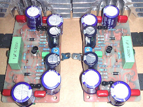
3. By dobrivoje:- Click >Here< (large onboard input film capacitor)
4. By John:- Click >Here< (old-school hand-drawn layout with curves)
5. By Damanhuri:- Click >Here< (Spacious layout with a lot of on-board PS decoupling)
6. By Olafk:- Click >Here< (Lovely Looking SMD PeeCeeBee)
Update(6/2/2013):
Some o'scope shots of PeeCeeBee performance:
1. By PMI:- Click >Here<
2. By nicos:- Click >Here<
3. By thimios:- Click >Here<
🙂
Update(19March2016): A couple new, improved and tested PeeCeeBee layouts have been uploaded. Links below.
Update(30December2016): PeeCeeBee V3 layout has been uploaded. The smallest yet the best sounding PeeCeeBee with 2"x2" footprint! Link below.
V1.1
Layout: >Here<
Pics:
V2
Layout: >Here<
Pics:
V3
Layout: >Here<
Pics:
(Old text from here)
Here is the VSSA all through-hole PCB as promised. (update- we now have our first SMD PeeCeeBee!
Check at the end of this post)Dimensions: 2" x 2.7".
There is no compensation capacitors and zobel on-board. If found to be necessary then the Zobel may be connected off-board at the binding post solder joints, and the Cdom(s) under the board between B and C of the VAS trannies. These accessories may find their place in the next version of the board, can't say for sure 😉.
The resistors marked OFF1 and OFF2 are to be left for fine tuning of the offset. A value of between 100K and 1M at any of these will set the offset very close to zero. These should be connected after the board is fully assembled with all the other parts. Ideally any one of the two resistors will be needed. If connecting on the positive side seems to increase the offset then leave that and concentrate on the negative side only.
The amp can be run from +/-15V upto +/-35V. The only part that needs to be varied is the default 15K resistors which are for 35V operation. I Use 10K for my 16V setup. This value is best decided through direct measuring of the VAS current at the 10ohm degenerators at their emitters. 10mA is a good bias, with small "U" shaped heatsinks for the VAS. Increase to 20mA if you can keep them cold by using better heatsinks. The trannies are aligned so that a single metal piece can be used for both. Don't forget mica insulator if this is your choice.
Pix of my finished and assembled boards:
If you have any queries about the board and setup etc. then feel free to post it here. I'll help as much as I can.
Happy listening.
shaan
edit:- The layout is in the VSSAbottom.pdf file.
Important:- Visitors/posters are welcome to modify any of the layouts according to their need and/or add totally new designs. However, if you want to use CCS or Multilayer Layout or Parallel capacitors in the feedback network then please post your VSSA experiment and results in the original VSSA thread. Link >Here<. This thread's topic is single layer printed circuit board designs based on the VSSA schematic without the above mentioned accessories, shown in one of the pictures attached below. Thanks for your co-operation.
Update(19/11/2014):
More Tested PeeCeeBee designs(kind contribution by fellow diy-ers):
1. By PMI:- Click >Here< (Pro-style layout with under-board MOSFET mount).
2. By Jason:- Click >Here< (TO3 output MOSFETs)
3. By dobrivoje:- Click >Here< (large onboard input film capacitor)
4. By John:- Click >Here< (old-school hand-drawn layout with curves)
5. By Damanhuri:- Click >Here< (Spacious layout with a lot of on-board PS decoupling)
6. By Olafk:- Click >Here< (Lovely Looking SMD PeeCeeBee)
Update(6/2/2013):
Some o'scope shots of PeeCeeBee performance:
1. By PMI:- Click >Here<
2. By nicos:- Click >Here<
3. By thimios:- Click >Here<
🙂
Attachments


Last edited:


Many Thanks Shaan! 🙂
Just 2 questions:
Why did you take out the CCS?
How much capacitance would you use with 35V rails?
Thank you again for your kind and good work!🙂
Just 2 questions:
Why did you take out the CCS?
How much capacitance would you use with 35V rails?
Thank you again for your kind and good work!🙂
Thanks all for the appreciation. I hope the design will serve its purpose.
Hi Paulo.
1. No CCS as performance is already excellent witout one.
2. About 15000uF per polarity for two channels.
shaan
Hi Paulo.
1. No CCS as performance is already excellent witout one.
2. About 15000uF per polarity for two channels.
shaan
Last edited:
I started to redraw peeceebee according to components I have in my drawer and found out that BD139 has wrong orientation. It must be reverted.
Indeed.
Pin orientation in TO126 devices like the BD pair is reversed from that of TO220 parts. So one needs to be careful, otherwise sharp clicks, chirps and pops will be heard.
Edit: in the silkscreen there are clear pin markers(c e for pnp vas and b c for npn vas) near the VAS bjts for avoidance of mistakes and to ease installation of either to126 or to220 parts, in case one opts for the latter.
Last edited:

Nice work! Dobrivoje...🙂
@ Shaan,
For ease of adjustment, is it possible to use v-trimmers in place of the offset resistors?
TY!
@ Shaan,
For ease of adjustment, is it possible to use v-trimmers in place of the offset resistors?
TY!
Nice work! Dobrivoje...🙂
No, no, I was not clear enough. It's my variant of shaan's peeceebee. I just moved some components to get space for big input cap and heatsinks for VAS transistors. I also tried to place all components on one quarter of Euroformat (160 x 100 mm) PCB. I'm still not satisfied, some tracks are too long, some components not at right places and yet shaan's peeceebee is better.
dobrivoje said:my peeceebee.
Looks cool. Which software are you using? I ask becaus my stupid-a** pcb making program lacks many popular models, like TO247/264. Thanks.
Shaan,
For ease of adjustment, is it possible to use v-trimmers in place of the offset resistors?
TY!
Of course. However, you wil need a 1Meg trimmer. Adding it to the board seemed to complicate the layout and increase board size by at least 10mm and demand two ugly jumpers. Aesthetix Lost. 🙂
It should be noted that without the off marked resistors it is possible to get an offset of less than 100mV. If this occurs then one only needs to connect a high value resistor(~220K) to either of the OFF marked spaces while keeping an eye on the millivoltmeter, this will ensure a very low and steady offset.
shaan
@naf
You're right. It's 100p. My mistake.
@shaan
I use free drawing program Free Graphic Design Software – DrawPlus Starter Edition from Serif
It's not PCB software, it's plain drawing program.
You're right. It's 100p. My mistake.
@shaan
I use free drawing program Free Graphic Design Software – DrawPlus Starter Edition from Serif
It's not PCB software, it's plain drawing program.
You will have to draw the new shapes yourself, but that's easy 😉Looks cool. Which software are you using? I ask becaus my stupid-a** pcb making program lacks many popular models, like TO247/264. Thanks.
You must have some instruction called "library add" or similar.
To know what they expect, put a similar component you already have (say, TO220) on the PCB and "disassemble" it, there must be some command which "turns it into primitives", which are the separate elements that make the symbol: pads, tracks, holes, labels, etc.
You draw your own in a similar way (remember elements will be in different layers) , select them, and add it to a library with a new name.
- Home
- Amplifiers
- Solid State
- PeeCeeBee