Working on it. I will post my final version along with my redrawn working schematic for peer review as soon as it is complete. If no errors are caught then I'll have a local print shop make me a film (I prefer photo resist, not much luck with toner transfer) and get a pair etched up.
Not sure I understand this post correctly? Parallel with the C1 input cap? So, in other words, The input cap should be 10uFd MKT in parallel with 2.2 uFd electro?One more very important info for all VSSA PeeCeeBee builders. Please install as best as possible 2,2 mF/6,3 V capacitor (Nichicon FG, Elna Silmic, etc) if possible paralleled with 10 uF/MKT (Vishay, Epcos, etc.).
Not sure I understand this post correctly? Parallel with the C1 input cap? So, in other words, The input cap should be 10uFd MKT in parallel with 2.2 uFd electro?
AC filtering cap at input bias current injection point: 2,2 mF ELCO parallel with 10 uF MKT connected to GND. In Shaan schematic these are two 1 mF elcos connected to GND I'm speaking about.
")
just for sake of clarity, 2.2 mF capacitor is 2,200µF, so the cap to ground has a value of 2,200µF (or larger) with a 10µF poly cap in parallel. Same for other parts of the circuit.
(If you want to write µ just keep the Alt key down and type 0181 on the number pad)
Thans for the tip cats squirrel. As we all know "u" is many times and mostly in use for micro sign and usually there's no big issue to understand the meaning, especially when speaking about electrical units, since that is commonly in use.
I would agree, but there have been times in the past when manuscript was sent to the publishers with the µ sign, but from a different font (symbols). Printers didn't have that font as standard, and the µ use to come out as m, along with all the confusion. At least, typing alt 0181 keeps it in the same font (usually), some fonts have different codes, though, so be careful.
A smaller value parallel cap with the 1000uF/2200uF feedback cap is not essential, like the matching of every symmetrical part of VSSA.
I see the paralleing as a luxory as it brought no audible benefit to me(it gave me fear of localized oscillation though, read esperado's posts in the VSSA thread.)
However, it's bound NOT to run into oscillation if the caps have very high ESR. But that means we have to use fastfood caps which can bring a plethora of problems like distortion from extreme non-linearity of dielectric.
Hence, the root of all confusion and uncertainity is eliminated: no parallel caps and a single expensive cap, per side.
Of course this doesn't mean you must not use a parallel cap, do if you wish. But please do not post it in the peeceebee thread, use the VSSA thread instead.
Humble request.
Thank you.
I misread your post (long week). So, increase the two 1000 uFd electrolytic caps to 2200uFd, and add 10uFd MKT in parallel, 6.3V.AC filtering cap at input bias current injection point: 2,2 mF ELCO parallel with 10 uF MKT connected to GND. In Shaan schematic these are two 1 mF elcos connected to GND I'm speaking about.
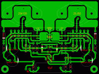
Peer Review Requested
Please see attached images and review for errors. The schematic shows BC547C/BC557C input devices that use a different pin-out than the 2SA965/2SC2235 I'm actually going to use (only because I have them), so don't let that misguide you, the pin-out I'm using is ECB.
Please see attached images and review for errors. The schematic shows BC547C/BC557C input devices that use a different pin-out than the 2SA965/2SC2235 I'm actually going to use (only because I have them), so don't let that misguide you, the pin-out I'm using is ECB.
Attachments
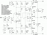
I assume you simulated the circuit? Main reason I ask is b/c I am wondering if there is anything in your model to account for a difference between gate capacitance of the two mosfets.
from http://www.sound.westhost.com/project101.htm:
...additional capacitors ... shown are to balance the gate capacitance. The P-Channel MOSFETs have significantly higher gate capacitance than their N-Channel counterparts, and the caps ensure that the two sides of the amp are roughly equal.
The VSSA is a very different animal from Rod Elliot's Project 101, so I'm not sure what Rod felt was required for his design directly translates to the VSSA. I used Bob Cordell's models for my simulations and did not find any issues with stability. The models used do account for the differences in the capacitances between the device polarities.
Other designs exist where there has been no specific need to match the capacitances of the N-channel and P-channel devices that seem to work just fine; just look at designs using vertical MOSFETs, the devices can be very different.
Other designs exist where there has been no specific need to match the capacitances of the N-channel and P-channel devices that seem to work just fine; just look at designs using vertical MOSFETs, the devices can be very different.
Hi Jason.
Peeceebee seems okay.
Just some points:
1) Use R1 in parallel with C2.
2) Try to draw a lone trace from GND to input "-ve", i.e. no other parts between input ground pin and main ground supply.
3) R18 is not necessary.
4) Decrease R12 and R16 to 10ohms and increase the two 15K resistors slightly to keep VAS bias same.
That was basically what I was wondering, thanks! Looks like a nice layout......The models used do account for the differences in the capacitances between the device polarities...

And, I did not mean to say that Rod's circuit is similar, but it just struck me that he found it necessary to compensate for that difference.
Please see attached images and review for errors. The schematic shows BC547C/BC557C input devices that use a different pin-out than the 2SA965/2SC2235 I'm actually going to use (only because I have them), so don't let that misguide you, the pin-out I'm using is ECB.
I'm not an expert (by far) and I haven't gone all the way through it, but I'm interested in this design as I do have a bunch of TO3 Hitachi's
Looks like nice work so far (to my uneducated eye). Just wondering if the low level grounds around the input should be on the same routes as the 1000 and 2200 uF capacitors? Could the lower level grounds be connected to the ground via 10 ohm resistors and parallel diodes in both orientations as seen on some other designs on this forum? May not be needed, but just a thought.
Thanks for doing this layout!
Steve.
ps. The values for R's 5-10 are not the same on the schematic and the pcb.
Last edited:
Hi Jason.
Peeceebee seems okay.
Just some points:
1) Use R1 in parallel with C2.
2) Try to draw a lone trace from GND to input "-ve", i.e. no other parts between input ground pin and main ground supply.
3) R18 is not necessary.
4) Decrease R12 and R16 to 10ohms and increase the two 15K resistors slightly to keep VAS bias same.
Shaan,
My input filters are arranged to avoid the voltage divider (attenuator) that the usual arrangement ends up being. I'd think it is still effective with two minor caveats - The base bias goes through both the 1k and 10k resistors and the input 'sees' the 10k in parallel with the sum of the 1k and the native input impedance of the amp, so a slightly lower input impedance. Still IMHO effective without sacrificing 10% of the input signal. If there is some other issue I'm not aware of my ears and mind are open.
The input grounding was something of a compromise due to limited space for traces. That said, my traces are fairly thick for the expected currents and I could likely go thinner to make one of the 1000uF cap terminals my audio ground or perhaps go all the way back to the ground spades. I was hesitant to go all the way to the ground spades because the input power is decoupled there, so the ground of one of the 1000uF caps seemed to be a better choice. Maybe I'm wrong...
The 100K at the input is simply to prevent the input from floating at a very high impedance. I agree it is not strictly necessary, but it is my preference to not allow the input to float.
R5, R10, R12, and R16 set the bias conditions and are interactive. I was experimenting with the values in simulation. Your advise is sound, it sims better with R12 and R16 at 10 ohm and R5 and R10 at 18k ohm.
Jason
I'm not an expert (by far) and I haven't gone all the way through it, but I'm interested in this design as I do have a bunch of TO3 Hitachi's
Looks like nice work so far (to my uneducated eye). Just wondering if the low level grounds around the input should be on the same routes as the 1000 and 2200 uF capacitors? Could the lower level grounds be connected to the ground via 10 ohm resistors and parallel diodes in both orientations as seen on some other designs on this forum? May not be needed, but just a thought.
Thanks for doing this layout!
Steve.
ps. The values for R's 5-10 are not the same on the schematic and the pcb.
Grounding is a sore spot on this layout due to the limited space. I could go thinner on the traces as they carry little current.
The 10 ohm with reverse polarity parallel diodes is a common ground loop breaker. I am not sure it is needed but if the room is available it could perhaps be included as a PCB option.
The R5-R10 values differ as the schematic was simply the values of my last sim and I labeled the PCB based on a hard copy I had from a prior sim. Sorry for the confusion. R5 and R10 set the bias current for Q1 and Q2 and the ratios of R7/R6 and R8/R9 set the gain. There seems to be some advantage to the lower values given the nature of the low impedance present at the summing nodes (the CFA variety this amp is billed as).
O.K. Thanks!I re-arranged the original placement of the input stage so that all the transistors that processes the +ve part of the signal remains above the ones processing the -ve part. To me this makes it look better and easier to digest.
- Home
- Amplifiers
- Solid State
- PeeCeeBee