My first version, which started from the same (Shaan's) schematic, is almost the same. My VAS heatsinks on that one are a bit smaller, VAS current is a bit lower, and the temp of the small heatsink reaches 47~55C - depending on the orientation of the main heatsink that my board is attached to. With no air circ., and fins flat on the table, that heatsink can raise the temp at the board 8-10C, compared to vertical position and off the table. When gauging temp by touch, that 10C can seem like z much bigger difference, if the temperature is at the comfort limit.Subjectively the transistors are pretty warm, but without any discomfort when touched and my contact-less thermometer says the VAS reaches about 45C...
I assumed the following:
max VAS current: 16 mA (tested)
max VAS suply voltage, after 1 diode drop: 36.5V (tested)
VAS heatsink rating: ~30C/watt
main heatsink rating: 0.65C/watt
max temp rise inside vented chassis: 15C (educated guess)
max room temp: 30C (assumed)
max VAS power at idle: 0.016A * 36.5V ~ 0.6W
(compare to KSC3503 in TO-126 package spec: 1.2W worst case derated)
worst case VAS transistor temperature:
max temp rise at VAS heatsink: 0.6W * 30C/W ~ 18 C
approx heatsink-to-case: 1.5~2C
Max VAS case temp: 30C + 15C + 18C + 2C = 65 C
Comparing to the Power Derating graph, not even half of the maximum after derating for case temperature.
Jason, is this about what you get when you look at the actual numbers?
@PMI
That looks about right to me and seems to jive with reality. Fact appears to be that even though the VAS seems warm there's still available margin with respect to thermal requirements. Unless VAS current gets WAY out of hand I don't think the average PeeCeeBee build will have any issues with typical TO-126 devices in the VAS.
My , and you get what you paid for
 ")
That looks about right to me and seems to jive with reality. Fact appears to be that even though the VAS seems warm there's still available margin with respect to thermal requirements. Unless VAS current gets WAY out of hand I don't think the average PeeCeeBee build will have any issues with typical TO-126 devices in the VAS.
My
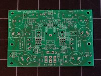
, and you get what you paid for Baked and out of the oven, Pee-Cee-Bee part duex.... (also known as Revision C of my through-hole layout).
In the last version, the main departure from the original layout was that I intended the trim pots, or at least one, to be permanently attached. Offset and bias adjustment using fixed resistors was (and is) still an option, although these are mutually exclusive with the trim pots. In other words, after the adjustment is made using the trimmer, it can be removed and a resistor soldered in its place.
The new version has a few more options, but can still be assembled according to the original schematic, with all conventional parts, and with no parallel film caps required... up to +/-35V supply, and 60~65W/channel with specified components. Some component values will change, mostly to accommodate higher voltage operation.
New in this revision:
For those who have my last board (or etched one), the distance between the mounting holes for the output fets is still the same, so the board will fit the same heatsink. If you want to mount VAS transistors under the board, two additional holes will have to be drilled and tapped.
The board was, and is, oversized compared to the others seen here. 70 x 102 mm or 2.75 x 4". Personal preference - if I am going to assemble something by hand, I like space between components... that way I can just make even bigger solder-bridges...
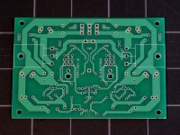
In the last version, the main departure from the original layout was that I intended the trim pots, or at least one, to be permanently attached. Offset and bias adjustment using fixed resistors was (and is) still an option, although these are mutually exclusive with the trim pots. In other words, after the adjustment is made using the trimmer, it can be removed and a resistor soldered in its place.
The new version has a few more options, but can still be assembled according to the original schematic, with all conventional parts, and with no parallel film caps required... up to +/-35V supply, and 60~65W/channel with specified components. Some component values will change, mostly to accommodate higher voltage operation.
New in this revision:
- Up to 100W/channel w. +/-45V supply, and 125W/channel w. component substitutions.
- More space for larger electrolytic decoupling and filter caps
- VAS transistors top-side or bottom mounted (at higher supply voltages)
- More space for bigger top-side heatsinks, or one common VAS heatsink
- Optional CCS (recommended above 35V supply voltage)
- TO-3P (Renesas latfets) or TO-247 (Semelab Alfets)
- Pads for protection diodes for ALF08P/N16-20
For those who have my last board (or etched one), the distance between the mounting holes for the output fets is still the same, so the board will fit the same heatsink. If you want to mount VAS transistors under the board, two additional holes will have to be drilled and tapped.
The board was, and is, oversized compared to the others seen here. 70 x 102 mm or 2.75 x 4". Personal preference - if I am going to assemble something by hand, I like space between components... that way I can just make even bigger solder-bridges...
Attachments
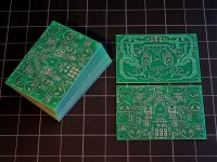
VSSA PCB made for through hole discrete parts
Hi PMI
So guys this is the VSSA PCB made for through hole discrete parts, released at just proper time, when VSSA PCB SMD group buy is going to be concluded.
This PCB should continue VSSA project and bring it to the masses all around the world.
PMI I am proud the PCB you've designed holds my acronyme, you have my blessing to go on with successful VSSA project.
Good luck!
Hi Guys, Thanks for the kind words. Would not have been possible without Shaan's ingenuity, and helpful comments from several other people.
Thanks for the kind words. Would not have been possible without Shaan's ingenuity, and helpful comments from several other people.Thanks, LC. I know you have been a big inspiration for at least a dozen diy efforts here. And thanks for the VSSA modules, which I really love....just proper time, when VSSA PCB SMD group buy is going to be concluded...
Yes, BC550C/BC560C, or same pinout, but other parts of your choice can be substituted. Q11 and Q12 are the optional CCS. With a resistor in place of that circuit, the board is electrically close to the one you built.Couple questions. Is the pinout for BC transistors? What are Q11,12?
Thanks Pete! Looking forward to building one of yours. I have been listening to Jason's all morning. I put the 18K's back in. After two hours of playing they are right at 235mv across the 10R resistors and measure 116F with my little infrared meter. This is with no case of course. If the heat will not hurt them I'm not going to worry about it. I won't be sticking my fingers in there
Blessings, Terry
Blessings, Terry
Perhaps not, but it will be, as soon as someone etches it himself, which is part of what makes it fun...@PMI , i don't think you PCB count as single layer even without trace on top layer
Didiet
edit:
Same thing applies to most of what I have been calling "options". It has almost all the features of Lazy Cat's V 1.4 schematic, but you can also just take Shaan's schematic from the beginning of this thread, some off-the-shelf parts, and you are good to go.
Last edited:
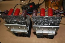
the double barrel is almost ready
Hi guys,
today I power it up, only 42VDC no higher yet because no more higher tap in the transformer.
What is the maximum voltage for 2 pair of K1058-J162?
I really want to use 55-60VDC if I can
@PMI nice boards, all in one board ...
the layout is easy to draw, even with hand drawing PCB.
(where is the pdf file btw?)
Now who will be the lucky one to try it first
Attachments
Hi Terry no problem, you are there in the sweet spot area...
Do you notice the sound maybe different now after some hour listening?
It should be some extra/hidden sound that maybe never heard before, more detailed sound?
My power supply not finish yet, but at my previous build the heat sink is quite hot but I can still touch them. I notice the heat sink is stable at that temperature so
don't worry about it if not too hot to touch (I forgot to measure the temperature at that time)
& they have a positive temp-co not like the BJT that need a VBE multiplier(negative temp-co)...
Because we bias it to optimal value it should be quite hot & the hotter they are the better it sound (but too hot is not good too).
We need to find our "sweet spot"
This new one have two pairs output so I can use higher voltage.
I also must find it sweet spot too, after I finish the power supply I will post again the result
Offset, bias, temperature, etc.
Regards
John
Last edited:
Thanks John. Yes, I can leave my finger right on the device. It is hot but tolerable. I figured it was OK but thought I would ask. I played it on 4ohm all day today. Sounds good. Gets a little crispy on the highs if pushed hard. May just be clipping. I'm driving it with an X-BoSoZ which is basically no gain. I drove 4425, 4412 & 4312 JBLs. All sounded good. I also drove some Event 20/20 nearfields. It really is a nice sounding amp.
Terry,
There's no issue with the output device temperature based on what you are experiencing.
I'm very happy to hear you are enjoying it and that I was able to be part of that.
It is possible that little bit of 'crispness' might be the slightest bit of clipping when you are playing loudly. Amps with lateral MOSFET output stages are not as voltage efficient (that is there's more 'loss') than amplifiers with BJT output stages. They simply can't get as close to the power rails. In this case you are 'loosing' anywhere from 8V to 12V off each rail, depending upon load. With your supply voltages the output should be clean to about +/-27V of output on your 4Ω speakers, so about 90W average output (to say RMS is a misnomer) maximum. I'm not too familiar with your speakers so I don't know how efficient they are, but that definitely plays a role as does their worst case impedance.
I know with my PeeCeeBee, running on +/-31.5V supplies into a nominal 6Ω speaker (that has an impedance dip down to just over 3Ω) with an efficiency of 93dB/W@1m can cleanly play to a level I will only tolerate for a couple of songs. Otherwise at 'normal' levels there is no issue, even with fairly dynamic materials.
Jason
Nice build John! (and thanks for the compliment). I think you are limited by the power and the current, and also the ability to keep the case temperature down, to stay below the power derating curve.Hi guys,
today I power it up, only 42VDC no higher yet because no more higher tap in the transformer.
What is the maximum voltage for 2 pair of K1058-J162?
I really want to use 55-60VDC if I can
Now why didn't you tell me that in the summer? I could have been finished by now!! "clown"@PMI nice boards, all in one board ...
the layout is easy to draw, even with hand drawing PCB.
I will post the layout when I am done testing.
Lazy Cat corrected me when I said something like that earlier in this thread, and after I looked at my test results and re-tested, I saw he was correct. It clips around 3V below the rails, and there is some distortion at about 4V below the rail. I will try to find the post. I could not test at full power, but clipping was tested....They simply can't get as close to the power rails. In this case you are 'loosing' anywhere from 8V to 12V off each rail...
With a 25V transformer at full power, ~35V DC supply, 31Vpk (~22Vrms) output, 60W into 8 ohms, 80W into 6 ohms (peak power only, because we most likely can't keep the outputs cool for long)
edit: found it
http://www.diyaudio.com/forums/solid-state/231662-peeceebee-57.html#post3518563
Last edited:
I will make a power supply board now...
the bare board already cut it's time to hand drawing some curves
Because my transformer not have a higher voltage output I will add one more transformer so the voltage must be more than enough
There will be 2 discrete bridge diode & six 10.000uF cap's
I hope 30.000uF per rail for stereo is enough, I'm planning to use CRC...
Regards
John
the bare board already cut
it's time to hand drawing some curves Because my transformer not have a higher voltage output I will add one more transformer so the voltage must be more than enough
There will be 2 discrete bridge diode & six 10.000uF cap's
I hope 30.000uF per rail for stereo is enough, I'm planning to use CRC...
Regards
John
- Home
- Amplifiers
- Solid State
- PeeCeeBee