Looking good!
Some non-critical, non-expert suggestions:
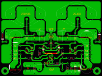
1) Could the two 1uF caps on each side be aligned to be parallel? (i.e. rotate the one sitting 'east-west' so they both sit 'north-south')
2) Could the trace from the 2000 uF cap up to the 1000 uF cap be thinner?
3) Is there enough room between the edge of the TO3 heatsink and the v+, V- and speaker out connectors?
Steve.
I'm no expert either, but here goes:
1) The orientation of those was a vestige from an earlier iteration and could likely be placed in parallel, if only for aesthetic reasons.
2) Why would you want any ground trace to be thinner?
3) I think so, there's .200" or 5mm clearance plus the connectors should be insulated anyway.
Thanks for the feedback.
And the difference with or without CCS-s is night and day?Very good VSSA PCB TO-3 you've designed jkuetemann.
Some day 18 k resistors will be replaced with CCS-s, believe me.
Regards L.C.
BTW it would be interesting to know which resistors have the bigest influence on sound.I want to replace cheap carbon resistors with something better like Vishay Dale but can't afford to change all of them...
Thanks LC!
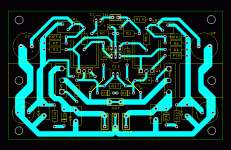
There's just a little cosmetic clean up to do but I think the last iteration posted will be very close to the final layout. I'll post the final version as soon as it is ready for peer review. If there's no errors I'm going to get a film made and etch up a pair.
Thanks for all the feedback, I think the comments I've received have definitely improved the layout.
Inspired by Jkuetemann's layout with all the power connectors in one place, I decided to do another pass on mine (well, w/o the cool and shiny TO-3's).
This time I tried it with the power transistors under the circuit board, and off to the side, gull wing style... I think I'll call that the DeLorean version (chuckle).
I allowed some extra room for two 10uFd MKT caps, and that pesky Zobel that messes up the nice symmetrical component placement. Also a bit more room for conventional heatsinks (25C/watt rating). The transistors are still close enough to mount on one strip of aluminum for thermal coupling, as an alternative to the two individual U-shaped heatsinks.
Which leads me to wonder how big a heatsink we really need?
The GIF resolution is not so good (sorry), but the layout was made in SPARK so it looks close enough for DIY.
And the difference with or without CCS-s is night and day?
Yes, on a speakers like this it is obvious like day and night.

(VSSA test on KEF R700 and 205/2)
")
Attachments
Hi fellows. 
The PeeCeeBee thread was opened to help the average diy-er adopt the symmetrical "current feedback" topology without introducing extra parameters like CCS, parallel caps, exotic (unavailable) parts etc. that aren't seen on simple "voltage feedback" amps, e.g. the P3A which is a marvel of its kind for the sonic benefit it provides with Such simplicity in the design.
VSSA, in its simplest form and minimal configuration that uses exactly six transistors in the whole amplifier is, and will remain the topic of this thread.
Thankfully,
shaan
... which is a marvel of its kind for the sonic benefit it provides with Such simplicity in the design.
VSSA, in its simplest form and minimal configuration that uses exactly six transistors in the whole amplifier is, and will remain the topic of this thread.
Thankfully,
shaan
Thanks Shaan to remind us all. Yes, this thread is dedicated to a symmetrical current feedback topology in its simplest form, to show what six transistors only can do, regardless any stability issues.

Also as we all can see this simple VSSA schematic triggered great creativity among forum members to design each its own PeeCeeBee, so very inspiring thread showing us all kind of approaches to the final solution.

I got my own too!
Today I got 2.25 dozen prints of the PeeCeeBee, based on the design in the first post. Looks pretty kool with the green mask on.
Populated one right away and it's singing, brilliantly. Offset 5mV without any manual setting.
26 more to go.
Pix will be uploaded soon.
shaan
Today I got 2.25 dozen prints of the PeeCeeBee, based on the design in the first post. Looks pretty kool with the green mask on.
Populated one right away and it's singing, brilliantly. Offset 5mV without any manual setting.
26 more to go.
Pix will be uploaded soon.
shaan
I got my own too!
Today I got 2.25 dozen prints of the PeeCeeBee, based on the design in the first post. Looks pretty kool with the green mask on.
Populated one right away and it's singing, brilliantly. Offset 5mV without any manual setting.
26 more to go.
Pix will be uploaded soon.
shaan
Can I get one pair of these boards?
No problem Shaan,The PeeCeeBee thread was opened to help the average diy-er adopt the symmetrical "current feedback" topology without introducing extra parameters like CCS, parallel caps, exotic (unavailable) parts etc. that aren't seen on simple "voltage feedback" amps, e.g. the P3A ...
all just all for fun here!I shall remove all the extra stuff presently. Just got carried away after reshuffling the parts around the power resistors under the board... (chuckle).
I consider myself to be a bit below the average DIY skill level anyway, LOL.
Thanks for the wonderful thread!
I got my own too!
Today I got 2.25 dozen prints of the PeeCeeBee, based on the design in the first post. Looks pretty kool with the green mask on.
Populated one right away and it's singing, brilliantly. Offset 5mV without any manual setting.
26 more to go.
Pix will be uploaded soon.
shaan
Please can I request you for a pair?
gannaji
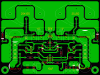
Same layout as above, with parallel capacitors, Miller compensation caps, and Zobel removed (to keep within the original intent of this thread).
For anyone else doing something similar, the component placement and track routing of this particular version in SPARK is pretty simple, either following the example provided above by Shaan, or with the power transistors mounted under the board, even using SPARK for the first time. If you already have Eagle, or other similar layout software, probably even easier...
Thanks to Shaan for starting this thread!
Attachments
Last edited:
My final versions
Fixed a critical error on the last layout presented, I had the input pair emitter connections swapped. I'm a little embarrassed that happened and somewhat surprised no one noticed. Also included a layout for the BC type input transistors. The pin-out of the BC's make a layout which is more straight forward. Since the BC547C/BC557C are higher gain than my 2SA/2SC that will likely end up the preferred layout, but I'm still going to give it a try with the Japanese transistors since I have them on hand. Sent out the image for a film to be made, so I'm hoping to be etching my boards this weekend.
Fixed a critical error on the last layout presented, I had the input pair emitter connections swapped. I'm a little embarrassed that happened and somewhat surprised no one noticed. Also included a layout for the BC type input transistors. The pin-out of the BC's make a layout which is more straight forward. Since the BC547C/BC557C are higher gain than my 2SA/2SC that will likely end up the preferred layout, but I'm still going to give it a try with the Japanese transistors since I have them on hand. Sent out the image for a film to be made, so I'm hoping to be etching my boards this weekend.
Attachments
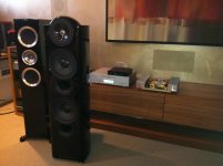
here's where my TO-3 version sits...
I don't like to think of the possibility the output shorted to +V or -V
- Home
- Amplifiers
- Solid State
- PeeCeeBee