I am just getting into learning the solid state end of thing, as my main area of interest has been valve guitar amps. I have found vacuum tubes to be way more intuitive learningwise, and really feel as if I'm a rookie again now that I am trying to give solid state a go.
I am currently going through bob Cordell's power amp book, and find that the Vbe multiplier is causing some head scratching.
I understand the basic concept of using the Vbe drop of the transistor to create the desired voltage at the collector end of the voltage divider. What is confusing me is exactly what voltage this is referenced to.
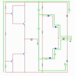
Let me ask this another way. On page 42 of bob's book, the basic amp schematic shows a 10ma current source hooked up to the +35 rail feeding the collector if the VAS transistor, who's emitter resistor is hooked to the -35v rail. The spreader is in series between them as seems to be the usual arrangement.
If the spreader wasn't there, what would the voltage be here? I feel it is intended to be at ground, or at least close for the spreader voltage to be correct on both ends, but even that doesn't quite work in my head. I see how the positive end is going to be correct, but shouldn't the negative end of the spreader be the same, only, negative? I just can't make it work in my head, and not being able to understand what the voltage would be at this node if there were no spreader makes it hard to even know where to start.
What am I missing here?
I am currently going through bob Cordell's power amp book, and find that the Vbe multiplier is causing some head scratching.
I understand the basic concept of using the Vbe drop of the transistor to create the desired voltage at the collector end of the voltage divider. What is confusing me is exactly what voltage this is referenced to.
Let me ask this another way. On page 42 of bob's book, the basic amp schematic shows a 10ma current source hooked up to the +35 rail feeding the collector if the VAS transistor, who's emitter resistor is hooked to the -35v rail. The spreader is in series between them as seems to be the usual arrangement.
If the spreader wasn't there, what would the voltage be here? I feel it is intended to be at ground, or at least close for the spreader voltage to be correct on both ends, but even that doesn't quite work in my head. I see how the positive end is going to be correct, but shouldn't the negative end of the spreader be the same, only, negative? I just can't make it work in my head, and not being able to understand what the voltage would be at this node if there were no spreader makes it hard to even know where to start.
What am I missing here?
The bias spreader, or amplified diode as is is also called, isn't referenced to anything. It floats effectively on top of the VAS output. If the bias spreader were not there the circuit would still function, albeit without any bias current and would exhibit much crossover distortion (let's assume the typical class B or AB output).
Basically, by flowing a current through the bias spreader it drops a specific voltage. One could suggest the top is referenced to its own bottom and it can be floated by the VAS to any level between the supply rails.
Basically, by flowing a current through the bias spreader it drops a specific voltage. One could suggest the top is referenced to its own bottom and it can be floated by the VAS to any level between the supply rails.
Ok, that actually helps a lot. Let's see if I have this straight. The spreader voltage basically rides along with the signal so that the output transistors on the positive swing always see the signal, plus the needed turn on voltage, ensuring that the output transistors conduct the whole swing from its zero point. Then, on the negative half, the signal is Less by the same amount for the same reasons.
So am I correct in that a DC operating point spice simulation will not necessarily give usefull results as far as the specific voltages at the spreader, but just that the voltages relative to each other matter?
While I now see that the absolute DC voltage at the VAS collector is not relevant to my question, it still bugs me that I don't know what quiescent DC voltage to expect at this node. If I eliminate the spreader and the output section, I am left with split supply rails which meet in the middle at the collectors of the current source and the VAS. My gut says there should be some predictable non-zero DC voltage here, but I can't figure out how to determine it if it even exists. This seems like it would cause an offset in the signal that would not be symmetrical in the output, so I really want to grasp this.
As AndrewT has mentioned, it is a type of voltage regulator. A two pin floating regulator with a temperature coefficient.
If you had no bias spreader or output stage, and you connected the NFB network to the VAS collector the amplifier would settle close to ground at the node where the VAS and CCS collectors are connected. Obviously in real life things are not matched perfectly and as such we get some small DC offset at this point. Add back the bias spreader, output stage and move the NFB take-off point to the output rail. Now the voltage at the VAS collector will be slightly negative, and at the CCS collector it will be slightly positive, each by about half of the spreader value. In real life these will be determined by the Vbe drops within the output stage.
The offset is more a function of how well matched and balanced the conditions are at the amplifier's front end. Unity gain DC NFB will set the output rail as close to ground potential as these inequalities allow. The polarity and magnitude of the offset could be estimated with analysis of the input stage. Also, one could expect without NFB in a typical amplifier an large DC offset or even going hard to one rail.
If you are trying to visualise what goes on, just think about a simpler alternative to a Vbe multiplier, bias spreader, amplified diode or whatever..... My gut says there should be some predictable non-zero DC voltage here, but I can't figure out how to determine it if it even exists. This seems like it would cause an offset in the signal that would not be symmetrical in the output, so I really want to grasp this.
the latest nickname for that variable bias controller circuit is. The circuit can be replaced by a string of diodes which also compensate for the
diode turn-on voltages in the output stage transistors. Say, for an EF2 design, you need an appropriate Vbias applied to the 4 Base-Emitter
junctions in series in the output stage. 4 diodes strung between the outputs of the VAS to the driver transistor bases will approximately do this.
These can also be attached to the heatsink to enable some thermal compensation in the equation, which is the other critical function of the bias
spreader for BJT and HEXFET output stages.
Many amplifier designs do use diode biasing but there are limits to their adaptability and compensation accuracy. That's why most now use the
adjustable and more sophisticated "bias spreader" circuits based on a cheap sensor transistor with a simple attachment to the heatsink.
If you are playing with simulation, the DC voltage to monitor as a reality check is that between the driver bases, Vbias, and this determines the
bias current in the output stage hence also Vre which is what we actually measure to set bias in the real world.
Last edited:
VBE multiplier is just a resistor...works alike a resistor that can sense the heat
works alike a termistor...just create a voltage drop of 2.4 volts considering the current you choice (darlington Emitter follower output)
Positive or negative is referenced by the output line that is zero volts...it gonna be connected through the speaker into the ground...speaker is 8 or 4 ohms... a low impedance to ground...output line is almost ground...it is zero volts.
How we have positive and negative?
Observe a emitter follower output (Dx amplifiers use emitter follower output)..observe there are junctions of base to emitter that are diodes.... two transistors represents two diodes in series...each diode has a voltage drop of 0.6 volts aprox.... so.... the two transistors you have upper the output line are posive...and the others goes negative referenced by the output line that is "almost" ground.
What "decides" were gonna be positive and were gonna be negative are these diodes because connected to the output line that is "almost" ground.
Transistor junctions have their limits..you cannot plug high voltage with the hope the junctions control the stuff... junctions overheat and goes shorted if you do that.... because of that we plug a resistor conducting a controled current inter connecting these diodes (base to emitter junctions).
Sorry.... i really want to help you..but my english is poor and does not help.
regards,
Carlos
Attachments
Last edited:
- Status
- This old topic is closed. If you want to reopen this topic, contact a moderator using the "Report Post" button.
- Home
- Amplifiers
- Solid State
- Help understanding bias spreader