I saved this one from the skip after someone tried to repair it before me it seems. I'd love to restore even if I'm not technical enough.
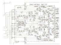
After some careful surgery to the PS I checked that it is OK. Not having a variac I connected it to 100Vac input through a step down transformer (it's a 240V model) and checked the power amp board for voltages. (Schem below). The voltages at the points shown on the schematic are proportionate to the supply input.
My problem (so far) is that when I check the voltage at the junction of Q1-Q3 and R13 (120K) one channel reads 0.67V and the other reads -5.6V. I have checked all transistors on that channel and replaced faulty ones with new, modern substitutes. I also changed C11 (330uF) on the faulty channel and checked 4 of the 'lytics around Q1-Q3.
After looking at the schematic attached can somebody please tell me what could be causing the faulty voltage reading.
Many thanks for your help.
Attachments
Check transistors Q1 and Q3 by measuring the voltage between the base lead and the emitter lead. A transistor that is working correctly will have a voltage of roughly 0.6-.7 volts. If one channel is operating correctly then cross checking the Vbe measurements for each transistor in its counterpart can help identify faults. You can check the voltage drop across diode junctions for the 0.6-.07 volts also. You can check all the transistors in this way as there may be other faults if in the one channel if previous repairs have been attempted.
Last edited:
Thanks mjona. Q1 was reading something like 5V. Removed and found 2 broken tracks. Out of curiosity I checked the transistor and found it OK (usual diode tests between pins) and checked its hfe which was >300. I thought I'd keep the original and soldered it again, taking care to join the broken threads to the nearest component on the same track.
When i checked the Vb-e again it was 0.15V. My question is is it possible for a good transistor to measure 0.15V instead of 0.6V between its b-e pins?
I'm asking because I don't want to solder in another transistor only to find that its Vb-e will be 0.15V again.
When i checked the Vb-e again it was 0.15V. My question is is it possible for a good transistor to measure 0.15V instead of 0.6V between its b-e pins?
I'm asking because I don't want to solder in another transistor only to find that its Vb-e will be 0.15V again.
The Base Emmiter voltage of a silicon transistor is between 0.6 and 0.7volts. If it is less it is turned off and the fault is most likely a balance problem on the output stage R43 R51 being too low as there is a problem with maybe a drive voltage. The output stage is complimentary and as such will be ballanced.
Q1 needs a bias current to flow in the path from emitter through the base to ground. There is a 100k resistor between base and this would normally go to ground - probably to adjust the output to the lowest d.c.voltage. In this instance there is a network of resistors and trimpots connected to that resistor.
Since Q1 emitter is connected through R13 to the positive supply rail and the base resistor and associated triming network needs to draw enough current to drop 0.6 volts across the diode junction of Q1 between emitter and base.
Assuming Q1 is O.K. as you measured a gain of > 300 then 0.15 volts suggests a maladjustment of the trimpot or a break of continuity somewhere in the chain or a changed value resistor or perhaps a worn trimpot.
You mention some broken tracks and resoldering some components to the nearest neighbour. If this is in the area of the trim network that might be suspect.
There should be a reading of 0.12 volts at R5 and the trimpot connection - if this is not true and you cannot attain that value with an adjustment to the trimpot you should check further in this area.
will the fact that this amplifier was running on 100Vac supply and not its designed 240Vac make any diffrence
I agree. Using a step down transformer isn't the best method imo. Use a bulb tester instead which will allow the amp to run on full voltage if there is no fault and limit the current if there is. The tranny does neither.
You will need to run the amplifier from 240 volts a.c. in order to be able to trim the d.c. offset under working conditions.
If you are concerned about possible damage during testing I suggest you check for any fuses in the amplifier power supply rails. If so you can remove them all (4 off) and replace the ones in the channel you are testing with a 100 ohm wirewound resistor of 5 watts rating.
I use a couple of these with small crocodile clips soldered at either end to bridge across the fuse holders. With these in place you can make all the voltage measurements necessary and these should be roughly consistent with those shown on the circuit diagram.
The problems you want to avoid is excessive current draw through the output stage through some fault and you don't want any excessive d.c. at the amplifier output.
The resistors will get very hot and very quickly if there is excessive current draw and you will need to switch off quickly. Having a finger on either resistor and another on the on-off switch will tell you what you need to know in that regard.
If there is no significant heat you can get the probes of your meter onto the ends of the resistor bridging the fuse holder at your leisure and deduce the current draw by measuring the voltage drop across the wirewound resistors - 100 ohms is a convenient value for ohms law, e.g. a voltage drop of 10 volts represents a current draw of 100 m.a.
From what you have described I expect you will find the d.c. offset is the more likely problem with the channel in question. If so that is where Vbe voltages and the biasing system referred to in my earlier post will play a part in determining the source of the fault.
Thank you all for your kind help and advice. R31 (10R 1W) was burnt and broken. I replaced it and this time I connected the amp to the mains with a lamp in series. The lamp glows brightly but soon after it dims down. I suppose this is as it should be so I tested the voltages as per cct diagram, and checked Vbe on all transistors (except outputs).
The results showed the voltages between the 2 channels were practically the same. So I inserted a pair of headphones and turned all switches and pots for some noise but it remained dead silent.
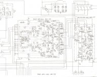
I must mention that since I first switched the amp on for the first time the protection lamp was on all the time and the Power lamp off. I thought the power lamp was broken and I decided to start checking the protection cct. The voltages at points 6 (-13V), 17 (7.5Vac) and 16 (35V) were as specified. However, at pin 14 (8V) the voltage was 35V; at the emitter of Q7 (7.5V) it was 0V. At Q5: coll = 10.8V; at emitter = 11.5V; at Q6-b it was 11.5V.
I removed Q7 (not the original) but its hfe measured OK.
I would appreciate any advice how to check and test the protection board, without causing damage to the power amp section. Should I disconnect the power amp board from the power supply? Or are things not as simple as that? What could be holding the protection circuit always ON? The output transistors were checked before starting and they measured OK.
Thanks and regards.
The results showed the voltages between the 2 channels were practically the same. So I inserted a pair of headphones and turned all switches and pots for some noise but it remained dead silent.
I must mention that since I first switched the amp on for the first time the protection lamp was on all the time and the Power lamp off. I thought the power lamp was broken and I decided to start checking the protection cct. The voltages at points 6 (-13V), 17 (7.5Vac) and 16 (35V) were as specified. However, at pin 14 (8V) the voltage was 35V; at the emitter of Q7 (7.5V) it was 0V. At Q5: coll = 10.8V; at emitter = 11.5V; at Q6-b it was 11.5V.
I removed Q7 (not the original) but its hfe measured OK.
I would appreciate any advice how to check and test the protection board, without causing damage to the power amp section. Should I disconnect the power amp board from the power supply? Or are things not as simple as that? What could be holding the protection circuit always ON? The output transistors were checked before starting and they measured OK.
Thanks and regards.
Attachments
Hi.
My eyes are not t0o good today im having a little difficulty reading the schem.. from what you say i believe R31 acted as a fuse . If the output devices are ok i would first be looking for a faulty semi not too much of a pita as only a few to check. You say pin 14 has 30 or so volts . Just to check is the pin 14 you mention on the left of the pwr amp scem.. If so im sure it should be conected to ground ??
My eyes are not t0o good today im having a little difficulty reading the schem.. from what you say i believe R31 acted as a fuse . If the output devices are ok i would first be looking for a faulty semi not too much of a pita as only a few to check. You say pin 14 has 30 or so volts . Just to check is the pin 14 you mention on the left of the pwr amp scem.. If so im sure it should be conected to ground ??
Last edited:
The protection circuit contains a single four pole relay which stops switch on and switch off noises getting through to both speakers.
It also prevents excessive d.c. getting to your speakers where the heat would pose a serious fire risk to the extend of losing your speakers and even having a house fire. A d.c. fault in either channel will prevent the relay from activating which is almost certainly the reason you are getting no sound on headphones.
As Mooly has pointed out, also alluded to by me, you need to quantify the d.c. voltage at the output of the faulty channel.
R31 has burnt out because too much current has been drawn through it and this raises the question of damage to transistor junctions through which this might have passed. There are two transistor whose collectors connect to R31 and these drive an NPN power device whose PNP counterpart was replaced at some time in history because of some fault and the NPN device may now be suspect.
You have replaced R31 but that has not cleared the fault so you need to know what level of current is passing through that now. Similarly you need to know what level of current is passing through the emitter resistors for the power devices.
You should be able to spot any problems by measuring the voltages across all these resistors, and comparing them with the circuit equivalents in the other channel.
If you would note these respective measurements and report your results it will help with further suggestions on solving your problem.
IMHO i believe the main cause of this fault can be found with the power off. All them voltage measurments on both boards pose a big risk at this stage it would be easy to end up with two dead channels as for the other channel it is only assumed to be working so can not realy be trusted as a good ref point..
Thank you all for your time and advice. Problem is I'm on and off on this job.
Seems I still have problems with my power amp section.
I've powered it through the series lamp to measure voltage at "pin3". It was -3.5V (quite off) while on "pin23" it was -0.12V. I also measured the voltage between the 2 complimentary pairs at "pin E" where it should be -38V. There the reading is 0V!! At the collectors (pins 36 & 27) the voltage is 37V which is very close.
You made me realise that pin 3 and 23 are the input to the protection circuit so it's beginning to make sense, at least logically if not technically. Now, how do I get pins 3 and 23 to 0V? VR3 and VR4 perhaps?
Thanks again for your help.
Your fault is almost certainly related to the driver transistors, possibly the outputs and related circuitry.
With the amp OFF you need to confirm that the following are OK.
D5 and D7 and the pot could be suspects as to the initial fault. You can apply a short (the blue line) using a piece of wire. The amp is safe to power up with this applied and will work correctly. This forces the output stage to zero bias current. The amp will still work and all the voltages can still be checked with it like this.
Attachments
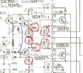
Pin E is an earthing point and there should be no connection with the power rails. There are decoupling capacitors for the power transistors between collector and earth. These are there for stability reasons.
You appear to have measured the positive rail on one channel for voltage with the negative rail on the other. 37 volts is not necessarily out of spec as some variation in mains could account for that. All four devices should register that +/- values at that level.
You will not be able to eliminate the -3.5 volt d.c. by adjustments to a trim pot. You can do that when you have eliminated the fault. You can then do both channels together. Minus 0.12 volts d.c. is somewhat out of spec but it will not cause any harm to your speakers.
In my experience in repairing d.c. faults the most likely cause is a problem transistor.
In addition to measuring the resistors and diodes in circuit with the power off you can check the diode junctions of the three transistors mentioned by Mooly under the same conditions.
In each of these there should be a forward diode junction between collector and base and between base and emitter. The junctions should conduct only in the forward direction. You will be able to use the diode check function on your meter for that.
You have three transistors in series and any may affect another in circuit and you may get some strange results especially if there is a fault. However if the other channel is working correctly which I think is the case the equivalent readings will be valid and you can cross reference the results to account for any disparities you find.
- Status
- This old topic is closed. If you want to reopen this topic, contact a moderator using the "Report Post" button.
- Home
- Amplifiers
- Solid State
- Help! Repairing a Pioneer SA-8100