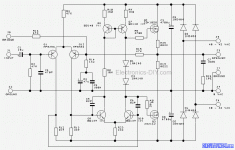
Hello,
I'm rather new to the amplifier world and I thought it'd be wise to present this circuit here, which is a design I've composed from bits and pieces scattered around the internet. I understand most of the stuff going on as my background is electronics technician, but it's been more than 10 years since I had anything to do with audio, which were a project we did back in school.
As said I've put this together from a lot of inspirational sources, for instance the VGS bias circuit originally only consisted of a potentiometer which made the quiescent current of the main power mosfets fly around like a mad onion in a thunderstorm when sweeping the temperature.
The OCP circuit was nicked from another design as well and seemed fairly idiot proof.
I've also added some clamping to the mosfet gates, I'm not really sure if it's necessary but it's of no harm.
I've simulated the hell out of the circuit, but I am a bit on unfamiliar ground as to simulating amplifiers, I've been trying to do all these mandatory THD plots, both with .four and with some nice add-on I found for spice - everything seems to be working nicely over a resonable temperature range.
So the reason I'm posting this is to get some feedback from the pros because I know that I can easily have missed "that circuit" or "that simulation" - Because this is my first project of this kind, and because I've spent a lot of time on it and nearly have the PCB layout done, I am pretty determined to stick with this design unless someone says "that design is notoriously known to open the gates of hell".
The powersupply is just a mockup in the simulation, just to get some more realistic picture of how it'd behave, I haven't decided on actual values or components for that yet.
The DC protection will most likely not be on the same PCB as the PA but rather on some output board.
So if you guys have any suggestions, things you'd recommend me to examine, simulate, additions etc. please let me know!
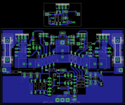
I've attached the LTspice file for anyone wanting to play around with the design, and also a picture of the layout, please note that the names of the components are not the same.
Thank you for your interest and help!
I'm rather new to the amplifier world and I thought it'd be wise to present this circuit here, which is a design I've composed from bits and pieces scattered around the internet. I understand most of the stuff going on as my background is electronics technician, but it's been more than 10 years since I had anything to do with audio, which were a project we did back in school.
As said I've put this together from a lot of inspirational sources, for instance the VGS bias circuit originally only consisted of a potentiometer which made the quiescent current of the main power mosfets fly around like a mad onion in a thunderstorm when sweeping the temperature.
The OCP circuit was nicked from another design as well and seemed fairly idiot proof.
I've also added some clamping to the mosfet gates, I'm not really sure if it's necessary but it's of no harm.
I've simulated the hell out of the circuit, but I am a bit on unfamiliar ground as to simulating amplifiers, I've been trying to do all these mandatory THD plots, both with .four and with some nice add-on I found for spice - everything seems to be working nicely over a resonable temperature range.
So the reason I'm posting this is to get some feedback from the pros because I know that I can easily have missed "that circuit" or "that simulation" - Because this is my first project of this kind, and because I've spent a lot of time on it and nearly have the PCB layout done, I am pretty determined to stick with this design unless someone says "that design is notoriously known to open the gates of hell".
The powersupply is just a mockup in the simulation, just to get some more realistic picture of how it'd behave, I haven't decided on actual values or components for that yet.
The DC protection will most likely not be on the same PCB as the PA but rather on some output board.
So if you guys have any suggestions, things you'd recommend me to examine, simulate, additions etc. please let me know!
I've attached the LTspice file for anyone wanting to play around with the design, and also a picture of the layout, please note that the names of the components are not the same.
Thank you for your interest and help!
Attachments
One suggestion would be to add a preset rather than using two diodes for a fixed bias. It doesn't need be temperature compensated for laterals.
Its not a million miles away from the old Hitachi application notes designs from way back. It should sound good.
Haven't looked at your files yet... maybe later")
Its not a million miles away from the old Hitachi application notes designs from way back. It should sound good.
Haven't looked at your files yet... maybe later
Hi Mooly,
Oops, I forgot to attach the schematic as a file viewable for others than LTspice users - the picture you commented on is the original one which very correctly just biases with two diodes, as you see in the attached I replaced those with a somewat thermally compensated solution
Oops, I forgot to attach the schematic as a file viewable for others than LTspice users - the picture you commented on is the original one which very correctly just biases with two diodes, as you see in the attached I replaced those with a somewat thermally compensated solution
Attachments
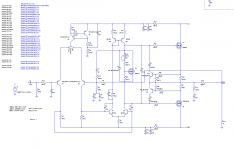
OK... so it looks like your changing the whole design around to try and use HEXFET's
Exactly
R23 seems to be far too high.
What about 220r?
But then R8 becomes too high.
D1 & 2 can be replaced with a variable resistor.
Have a second look at R3 value.
Add Zener protection for the gates.
Add RF attenuation.
Re-look at C1:C2 ratio.
Hi AndrewT,
I'm sorry for the confusion, please find the updated schematic and ltspice file in the last post, I took your advice regarding the capacitor ratios, I can see the sense in that
Sorry.Hi guys,
I just updated the schematic, added the clamping on the gates and changed the decoupling capacitor in the FB to the same value as the input one (c2 and c3).
Never mind.
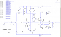
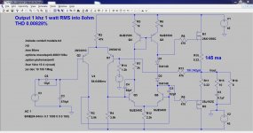
I've just done a quick sim of the circuit in post #1 for a starting point using laterals. The circuit as is doesn't run and the output sticks at the rails. R8 (10K) is the culprit. Its too high. Anything below 5 k runs and the amp works OK. I haven't time tonight to look at anything else on it but I will be interested to see how it performs, how it performs lateral vs HEXFET and how it compares to a new design I'm just toying with
Attachments
I've just done a quick sim of the circuit in post #1 for a starting point using laterals. The circuit as is doesn't run and the output sticks at the rails. R8 (10K) is the culprit. Its too high. Anything below 5 k runs and the amp works OK. I haven't time tonight to look at anything else on it but I will be interested to see how it performs, how it performs lateral vs HEXFET and how it compares to a new design I'm just toying with
It's interesting with those poorly translated to english sites where I found that circuit, it seems as if they, in general, deliberately screws something up in the design so that it doesn't work, I've seen lots of designs where one of the output transistors have drain source/collector emitter swapped for instance, with this design it's the resistors...
It's a nice circuit, I really like the simplicity of it, regarding laterals for this circuit wouldn't it just be a matter of biasing them with a different voltage or how?
Why would you choose laterals and not hexfets, something with distortion?
Some quick sims here for anyone interested. It might be possible to greatly improve on the performance but as it stands its not good. Seems to be a lack of current drive for the gate capacitance of the FET's for one thing.
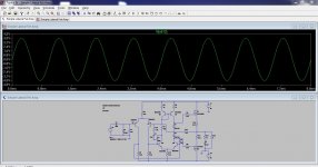
You asked earlier about choosing Laterals... well for me they are the device of choice for output stages Last two plots show a lateral design.
You asked earlier about choosing Laterals... well for me they are the device of choice for output stages
Last two plots show a lateral design.Attachments
-
 Lateral FET 1Khz Circuit.JPG154.5 KB · Views: 55
 -
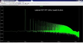 Lateral FET 1Khz FFT.JPG205.6 KB · Views: 53
 -
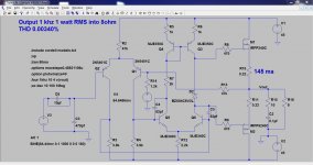 HEXFET 1Khz Circuit.JPG152.9 KB · Views: 53
 -
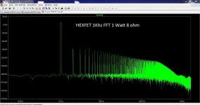 HEXFET 1Khz FFT.JPG205.4 KB · Views: 56
 -
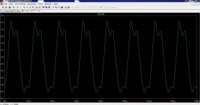 Squarewave 50Khz.JPG122.9 KB · Views: 28
 -
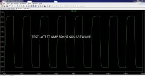 Test LatFet Amp 50Khz Squarewave.JPG182.2 KB · Views: 29
 -
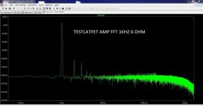 Test LatFet amp FFT.JPG174.7 KB · Views: 32
- Status
- This old topic is closed. If you want to reopen this topic, contact a moderator using the "Report Post" button.
- Home
- Amplifiers
- Solid State
- Simple amp