Hello all!
With a few pairs of Sanken, I decided to make a card for the P3A class A.
I do not know if the design of the circuit is optimized properly but I have found no connection error.
For those interested I have attached the files.
Greetings!
With a few pairs of Sanken, I decided to make a card for the P3A class A.
I do not know if the design of the circuit is optimized properly but I have found no connection error.
For those interested I have attached the files.
Greetings!
Attachments
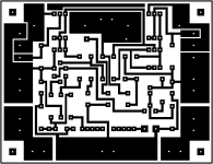
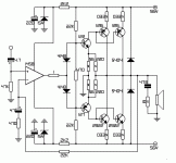
You are pushing the stability envelope using very high Ft output parts in a CFP ouput stage.
That's risky but to compound this with long, wandering traces of inappropriate and strangely
varying thickness there is asking for trouble. You can do a lot better there in the physical location
of the drivers and placing the output transistors along the same edge to get the traces to more
reasonable length. Lead stress due to mechanical assembly issues will likely be reduced too.
There are several threads here of guys DIYing their own P3a PCB which is fine as a learning exercise,
so please search those P3a threads for the hard lessons and good advice in PCB layout first.
This topic comes up again and again so it's not just a matter of one opinion.
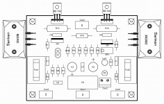
I changed the design in the hope that here will be better. The drivers are now two transistors coupled to the transistor by a thermometer aluminum plate serving as a heat sink.
Thank you for your contributions!
Thank you for your contributions!
Attachments
Last edited:
Hello all!
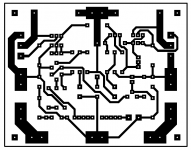
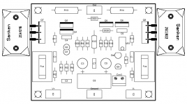
I tried to improve the design of the card, but I have a small question.
The first image track passes between the legs of the transistor Q8 but I think it is very close.
On the second picture I put a strap.
What is the best design?
Thank you!
I tried to improve the design of the card, but I have a small question.
The first image track passes between the legs of the transistor Q8 but I think it is very close.
On the second picture I put a strap.
What is the best design?
Thank you!
Attachments
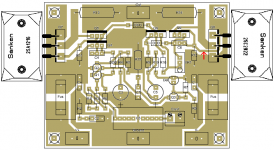
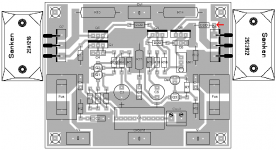
The second one, if you are making the PCB at home and have no soldermask.
Q9 should not be a TO-220 device... an MJE340 (TO-126) will be OK though.
In this design, and especially with those Sankens, i would recommend extra 330uF decoupling capacitors in parallel to C+ and C- for stability.
Q9 should not be a TO-220 device... an MJE340 (TO-126) will be OK though.
In this design, and especially with those Sankens, i would recommend extra 330uF decoupling capacitors in parallel to C+ and C- for stability.
What about this project?Hello all!
I tried to improve the design of the card, but I have a small question.
The first image track passes between the legs of the transistor Q8 but I think it is very close.
On the second picture I put a strap.
What is the best design?
Thank you!
I'm interesting because i have 2sa1295 2sc3264.
")
I did not continue this project in doubt and I preferred to use my Sanken in the DX Super A destroyerX.
http://www.diyaudio.com/forums/solid-state/221741-dx-blame-st-together-dx-super.html
regards!
http://www.diyaudio.com/forums/solid-state/221741-dx-blame-st-together-dx-super.html
regards!
What the result with that sanken 2922/1216?
I have them also
but I doubt it will suit in this tricky circuit...
on the original site no recommendation to use it, maybe can cause some trouble
these are the words( tricky circuit ) coming from the mouth of someone that doesn't understand the principal of operation of an sziklai amplifier and further more the benefits that come with .
Absence of this understanding and some failed sziklai hi power designs gave a wonderful amplifier a bad reputation ...
Proper drivers ,with proper compensation , with proper bias , proper procedure, adjustment,proper methodology when amp is ready to evaluate and measure and any transistor of your choice is suitable ....you just need to know ( like any other amplifier )how to operate it properly
Kind regards
Sakis
Last edited:
DX
almost! Just assemble the cards with the power and go to settings.
Regards!
good luck .
Are you finish it?
regards
almost! Just assemble the cards with the power and go to settings.
Regards!
forword your experiences.almost! Just assemble the cards with the power and go to settings.
Regards!
best regards.
Hi Sakis,these are the words( tricky circuit ) coming from the mouth of someone that doesn't understand the principal of operation of an sziklai amplifier and further more the benefits that come with .
Absence of this understanding and some failed sziklai hi power designs gave a wonderful amplifier a bad reputation ...
Proper drivers ,with proper compensation , with proper bias , proper procedure, adjustment,proper methodology when amp is ready to evaluate and measure and any transistor of your choice is suitable ....you just need to know ( like any other amplifier )how to operate it properly
Kind regards
Sakis
have you try this MT-200 type in your P3A, I would like to know
& yes, I don't know much about sziklai output but
I have try it in another amp circuit with opamp & yes it is different sound but has oscillation problem.
I don't even know how to make it work good, I have not good education on this also I don't have such a good equipment for make proper amp.
One question if you don't mind
would you suggest me to try it with this sanken & some precaution please
Kind Regards
John
No ... i have never try MT 200 devices for a P3A amplifier for a number of reasons
A) obviously using these transistors for a P3A amplifier is an absolute overkill as those are designed for much higher power amplifiers
B) I like to run my semis as close is possible to the limits cause i think that this way i get the best of them then again MT 200 is out of the question ( the rule actually applies to all the rest of the transistors except outputs though the concept remains the same )
Dummy load with capacitive function + gen + scope and far better a spectrum will tell you all the truth about it ..
IC + sziklai output stage rings a bell ...The Chameleon HILL one of the biggest sziklai failure The amplifier had huge construction errors still it could simulate quite well
Obviously oscillation will occur from bad compensation, poor pcb design , inefficient decoupling and poor filtering ,
as about your previous IC+ sziklai schematic i d'like to see a schematic as for the P3A +MT 200 some day in the feature i will make a test and post my results in my thread about the P3A
--------------------------------------------------------------------------------------------------
Allow me to add 2 cents
If one manages to understand the principal of operation in an EFP and a CFP amplifier the next question will be ( always ) "what if i need mo Power ??"
For an efp is almost a walk in the park and increasing rail voltage use higher voltage semis and parts and multiply the outputs and you are almost done
many weapons available ..current sinks / mirrors , diamond LTP , double VAs , Cascaded VAS ... For an EFP most of the times this will mean that the amp will preserve most of the characteristics only produce much higher power
Our forum actually is full of schematics based on the above concept In reality though very few "designers " less than 10-20 produced a schematic that is almost idiot proof or its simply dressed up with the proper calculations and safety measures to operate properly and safe at this range of power .
( yes this a reminder of my complain that work around known protection like VI limiters is stopped very long time ago proper implementation never existed or totally stopped )
Increasing rail voltage in CFP amplifier together with adding more outputs is a very poor choice and it might increase the current available from the output stage but will not preserve the characteristics of the amplifier .
The output stage in an SZIKLAI will work on its own and yes it will fall to oscillation if working in high voltage and many parallel outputs . there is stability measures to be taken and often these will work from the aspects of safety but all the sound of an SZIKLAI will be gone ,,,
Closing argument
As well know my theory is poor so i cannot help much with simulation and calculation most of these nice information come cause i only work with the P3A for the latest 6 years .
To my understanding or with known technology an sziklai amplifier cannot be made with more than two outputs there was efforts to make CFP amplifiers with double drivers and double outputs = double CFP outputs or CFP biased in class A ,free of oscillation problems but not any better than any EFP amplifier
Due to the nature of sziklai and the percentage used ( something like only 2-5 % of amplifiers made commercially was cfp ) i think that the circuit is not investigated to it's full potential ... Who knows some time in the feature it might happen
KInd regards
Sakis
Ok, I will wait what your finding next...IC + sziklai output stage rings a bell ...The Chameleon HILL one of the biggest sziklai failure The amplifier had huge construction errors still it could simulate quite well
Obviously oscillation will occur from bad compensation, poor pcb design , inefficient decoupling and poor filtering ,
as about your previous IC+ sziklai schematic i d'like to see a schematic as for the P3A +MT 200 some day in the feature i will make a test and post my results in my thread about the P3A
KInd regards
Sakis
actually I never build P3A before,
but after saw your thread & it's potential maybe I'll try it
I will have more new experience with
SziklaiThanks for the explanation above
Attachments
the schematic shown above i s a horrible effort of someone that seen a generic schematic i memory serves from RED circuits where a simple op amp drives a couple of transistors for a low power and lo fi application .
Someone did the mistake described above increasing rail voltage and number of outputs expecting that this will work ...For this circuit you have no chance with an sziklai output scheme ... if you choose to go with EFP this will work only 10% better ...
With this drive you simply have no chance
kind regards
sakis
I'm fully agreeWith this drive you simply have no chance
I'm really sorry for posting that schematic,
I was build it & you know that I'm fail
bad story
& I'm a bad guy that don't know much about designing ampI'm here to learn from experience, from myself or from you guys
P3A will be another story,
well I will try it just wish me it can work properly
need to reread your thread again to see some important clew
I have a pair 2SA1302-C3281(green& black) bought around 2000 was used in other amp @ +/-45VDC rail
I hope they are not fake... the back are shinny
A1941-C5200 maybe the first to try, then maybe MJL21193-21194 or then Sankens
Sakis, one more clew of the original toshiba you have, picture please if you don't mind
Thanks
- Status
- This old topic is closed. If you want to reopen this topic, contact a moderator using the "Report Post" button.
- Home
- Amplifiers
- Solid State
- Rod Elliott P3A with SANKEN 2SC2922/2SA1916