First of all: I don't have much experience with solid-state amplifier circuits or SPICE simulation. I'm interested in the 50W amplifier circuit shown on this website:
2N3055 50W Audio Amplifier
After downloading the SPICE models for the transistors and op-amp IC I wanted to simulate the circuit with LTspice IV.
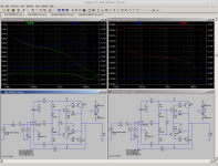
After running the simulation on the original circuit, one can notice a difference in the output transistors' Collector currents. Especially at high frequencies (>3 KHz) there is a big difference.
I also simulated the circuit with transistor types that are (much) more easily available for me; 2N2222 & 2N2907 as driver devices and BD243 & BD244 as output devices. This time there is no high frequency increase in Collector currents, but the 0.8 A difference remains.
I wonder if this would be a feasible design for a simple solid-state amplifier. Perhaps BD243 & BD244 pair could be used at lower supply voltages and output power?
LTspice circuit files are attached.
2N3055 50W Audio Amplifier
After downloading the SPICE models for the transistors and op-amp IC I wanted to simulate the circuit with LTspice IV.
After running the simulation on the original circuit, one can notice a difference in the output transistors' Collector currents. Especially at high frequencies (>3 KHz) there is a big difference.
I also simulated the circuit with transistor types that are (much) more easily available for me; 2N2222 & 2N2907 as driver devices and BD243 & BD244 as output devices. This time there is no high frequency increase in Collector currents, but the 0.8 A difference remains.
I wonder if this would be a feasible design for a simple solid-state amplifier. Perhaps BD243 & BD244 pair could be used at lower supply voltages and output power?
LTspice circuit files are attached.
Attachments
Hi,
This thread details a similar but better design :
http://www.diyaudio.com/forums/solid-state/54448-rega-brio-one-channel-dead.html
More designs of the type here :
A Paul Kemble web page - PW Texan amplifier and the PE Rondo.
rgds, sreten.
This thread details a similar but better design :
http://www.diyaudio.com/forums/solid-state/54448-rega-brio-one-channel-dead.html
More designs of the type here :
A Paul Kemble web page - PW Texan amplifier and the PE Rondo.
rgds, sreten.
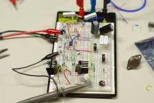
I built a breadboard prototype and the circuit seems to work. I used two lab power supplies to to power the circuit and performed some analysis using an oscilloscope. I changed the value of resistor R9 from 10R to 470R and noticed a 10dB reduction in levels of the harmonic "spikes".
Circuit:
Output voltage into a 10R/5W resistor
R9: 10R,
R9: 470R,
FFT analysis of output:
R9: 10R,
R9: 470R,
Circuit:
Output voltage into a 10R/5W resistor
R9: 10R,
R9: 470R,
FFT analysis of output:
R9: 10R,
R9: 470R,
Attachments
Last edited:
Member
Joined 2009
Paid Member
you don't just simulate but you build, you measure and compare. That gets +1 from me.
Interesting output stage design. The waveforms in your last simulation look really awful. My preference is still for the double emitter follower where Q1 and Q2 collectors are taken to their respective supply rails and the junction of R10 - R11 is not grounded but floating.
Interesting output stage design. The waveforms in your last simulation look really awful. My preference is still for the double emitter follower where Q1 and Q2 collectors are taken to their respective supply rails and the junction of R10 - R11 is not grounded but floating.

Dunno about the author of the first schematic linked in #1 but their parts list was out of date in about 1970. 2N2222/2N2907 are are also dinosaurs used as generic/default parts in simulators and Radio Shack. I guess any silicon will function in a crude audio amplifier but these parts are not well suited to audio. You would have to dig through really prehistoric stock to find 2N3053/2N4037!
Try to locate more credible sites and designs before wasting your time and money on the mediocre, ancient parts and ideas that would be better as static museum exhibits. We have plenty of threads and designs to search that will sweep these away in any performance categories you care to name. So does ESP and other reputable audio design/forum sites, for that matter.
Try to locate more credible sites and designs before wasting your time and money on the mediocre, ancient parts and ideas that would be better as static museum exhibits. We have plenty of threads and designs to search that will sweep these away in any performance categories you care to name. So does ESP and other reputable audio design/forum sites, for that matter.
I have designed many amps with this topology. Why many? Because this is not a plug and play circuit. Different opamp, different circuit. Different driver, different circuit. Different output stage, different circuit. The topology is not safely stable. This is a classic topology and you will find many failed amplifiers using this. If you want to use it, a protection scheme must be used.
Slow parts (741) must go with slow parts (3055), fast with fast.
The issue with this topology is that it requires strict operating condition. This is not a simple issue if our simulation models are not precise and we don't have proper measurement tools. Because our amp, even tho working, may have instability issue such that we must implement the protection circuitry to be safe.
Well, the fact is, the rate of failure of this topology is very high, whichever the circuit.
I like this topology because it is where slow parts can sound good. Instrumentation opamps are slow but often good sounding and can be used here.
It's a (CFP) buffer with gain . You need gain because you need to bring your maximun +-15 V signal coming out from the OP-Amp to output rails level.
This configuration, as many said (also there is an article on the ESP site) may work if well executed, but is troubleful to stabilize. Maybe you should consider to add a normal VAS stage and bring back the gain of the buffer to 1.
Interesting experiment, though.
This configuration, as many said (also there is an article on the ESP site) may work if well executed, but is troubleful to stabilize. Maybe you should consider to add a normal VAS stage and bring back the gain of the buffer to 1.
Interesting experiment, though.
Last edited:
I'm very interested in hearing about your project! Notes and suggestions would be very welcome if you have some free time.I was able to make a very high quality version of this amplifier, I will see if I can find the notes and post some suggestions when I have some more time after work.
Thanks for your suggestion. I agree that the waveform is very awful. I made some experiments by arranging the output transistors into a Darlington configuration. Is this what you meant?you don't just simulate but you build, you measure and compare. That gets +1 from me.
Interesting output stage design. The waveforms in your last simulation look really awful. My preference is still for the double emitter follower where Q1 and Q2 collectors are taken to their respective supply rails and the junction of R10 - R11 is not grounded but floating.
http://sound.westhost.com/articles/cmpd-vs-darl.htm#s6


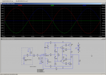
I also tried modifying the original circuit slightly, by changing the values of R5 and R8 to increase the current going through the diodes. The graph shows the output voltage into the 8R resistor and the base currents of driver transistors.


Thanks for your comments
I made the small tweak of changing the values of R7 & R8 by paralleling them with 22k resistors. So the total resistance ends up being (15⁻¹ + 22⁻¹)⁻¹ = 8.9k.
It was surprising to see such a big difference in how the waveforms appear on the oscilloscope. Especially the magnitude of sharp harmonic peaks was reduced in FFT analysis.
Here are some more pictures.
Driver transistors' base voltage levels (the channel connected to PNP is reversed in display):

Voltage across NPN driver transistor's 47R emitter resistor:

Voltage across PNP driver transistor's 47R emitter resistor:

FFT analysis of the output into 10R/5W resistor:

2x zoomed view of previous:

FFT of amp driven heavily into clipping. I only used +-200mA limited power supply as the output transistors only have tiny heatsinks, I don't want to fry them:

I still need to experiment with the Darlington configuration and a better constant-current device than a resistor. Maybe also try to implement some kind of short-circuit protection circuit with a 2N3904&2N3906 pair.
It was surprising to see such a big difference in how the waveforms appear on the oscilloscope. Especially the magnitude of sharp harmonic peaks was reduced in FFT analysis.
Here are some more pictures.
Driver transistors' base voltage levels (the channel connected to PNP is reversed in display):
Voltage across NPN driver transistor's 47R emitter resistor:
Voltage across PNP driver transistor's 47R emitter resistor:
FFT analysis of the output into 10R/5W resistor:
2x zoomed view of previous:
FFT of amp driven heavily into clipping. I only used +-200mA limited power supply as the output transistors only have tiny heatsinks, I don't want to fry them:
I still need to experiment with the Darlington configuration and a better constant-current device than a resistor. Maybe also try to implement some kind of short-circuit protection circuit with a 2N3904&2N3906 pair.
Last edited:
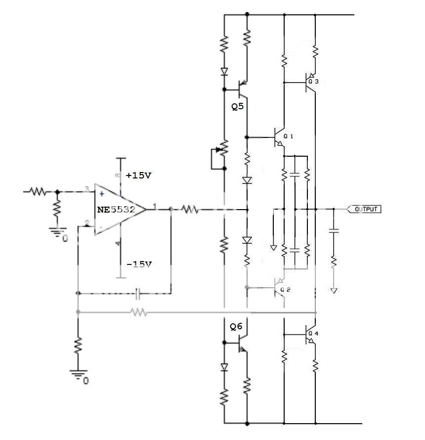
Q5, Q6 make up a CCS for the bias of Q1, Q2. We want to run about 2mA through the the diodes biasing up Q1 and Q2. I used MPSA06/56 for all the small signal types, others may be suitable. The MPSA06/56 are rated at 500mA max collector current, so they have plenty of muscle to act as drivers for the outputs, they are also available in 1W types (the MPSW06/56 if you want to bias them real heavy. I think I ran about 4mA through Q1 and Q2, with 51Ω as their emitter resistors to ground, I used 150Ω feedback resistors to the output, and the caps were about 10nF.
The outputs were TO220 versions of the 3055/2955 and they were mounted with no insulators on a common heatsink, one for each channel. A TL072 was tried, but the NE5532 sounded vastly better so we bit the bullet as far as the increased cost, the TL074 were used elsewhere. The Zobel was the usual 10Ω and 100nF. The amplifier was deliberately overcompensated and had a bandwidth of about 250Khz. We used a 160VA 20-0-20 transformer to power the two-channel version, it sounded much beefier than the original 80VA we had planned on.
The outputs were TO220 versions of the 3055/2955 and they were mounted with no insulators on a common heatsink, one for each channel. A TL072 was tried, but the NE5532 sounded vastly better so we bit the bullet as far as the increased cost, the TL074 were used elsewhere. The Zobel was the usual 10Ω and 100nF. The amplifier was deliberately overcompensated and had a bandwidth of about 250Khz. We used a 160VA 20-0-20 transformer to power the two-channel version, it sounded much beefier than the original 80VA we had planned on.
The hand-wired prototype was evaluated with pure class B bias in the outputs, ie: none. This was done to eliminate any bias adjustment in the production line. I deliberately did not tell anyone this as "everybody knows class B doesn't sound good". The amplifier was evaluated on some very expensive speakers done by a top designer and everyone was stunned by how good it sounded, going so far as to bring in their own high $$$ hi-fi amplifiers only to find them suffering by comparison. Keep in mind this was designed for a computer sound system and fit into a half-height drive slot (external transformer). The product was shown at the Comdex Show in Las Vegas in 1997, and marketed as an OEM product to many different PC manufacturers.
Last edited:
I finnally finished a concept with discrete current feedback opamp on this configuration, slightly modified into compound type exit. You cannot imagine, how high is level of quality of reproduction on complex RLC load via my old HP oscilloscope and sweep of Wavetek 182. But there are many years (10) of elaboration and tests. There are also very good measure to made this concept with IC's directly, but with used mirror type active feedback for more quality phase response.
- Status
- This old topic is closed. If you want to reopen this topic, contact a moderator using the "Report Post" button.
- Home
- Amplifiers
- Solid State
- 50W BJT amplifier