I im designing a new amplifier and found this interesting article:
Memory Distortion Philosophies - Part 4 : Circuits
As from the link i would like to simulate this input stage in LTSPice...and if anyone could help me how to simulate for now only input stage(Linearity, Gain, SlewRate, THD, etc...)
here is example input stage only with bjt:
https://sites.google.com/site/fabaudio/input_stage_low_mem.jpg
As you can i add p-jfet and n-jfet to bjt. Together i get all the benefits from bjt and jfet so linearity need to be perfect.
For jfet i have choose 2SK170/2sj74 from Toshiba
For bjt i have choose 2SA970/2SC2240 from Toshiba
Between Resistors R3/R4 it must go to CCS Source, and from J1/J2 Drain it gets to Current Mirror With Two Bjt Transistors (2SA970/2SC2240).
What do you guys suggest to be the best CCS Source and Current Mirror or should i use other suggetions?
I im attaching LTSpice file with schematic if someone could add commands to simulate only this input stage and uplodad it here so we can discuss here what is better and to fine tune this input stage (High Linearity, Slew Rate...)
Many Thanks.
And if someone can add models Toshiba 2SA970/2SC2240 and JFETs (2SK170/2SJ74 Toshiba).
An externally hosted image should be here but it was not working when we last tested it.
Attachments
Member
Joined 2009
Paid Member
There is a serious problem with the memory distortion for me, which makes it difficult to consider the extra complexity. The premise and the theory is good. But the CFP and the casdoding both significantly improve the performance of the circuit even if there is no memory effect at all. So when comparing the simple single device with complex circuit you can't separate out what improvement is from elimination of the memory effect and what is simply a much more linear circuit. So for me, there is no evidence that improvements are due to reduction of memory effect.
Member
Joined 2009
Paid Member
Hey I wasn't saying that the design you are looking at is bad, in fact it looks to be pretty high end to me with good linearity. I'm just saying that I didn't see evidence that memory distortion is an issue. I think the input stage you posted can stand on it's own feet without reference to memory distortion, it is a very worthy design.
Are there better input stages ? - I'm not sure, but there are several on the forum that also look good. I can't say if one is best.
Are there better input stages ? - I'm not sure, but there are several on the forum that also look good. I can't say if one is best.
Generally speaking, BJT's are great for driving the source of a common gate J-fet amplifier. Driving the source with a dependent current source (collector) mitigates the non-linear changes in Vgs vs Id. In fact the VAS of the stereo module I made is complementary common gate J-fet.") But, I recomend that the next stage be buffered or have a high (AC) current gain.
But, I recomend that the next stage be buffered or have a high (AC) current gain.
But, I recomend that the next stage be buffered or have a high (AC) current gain.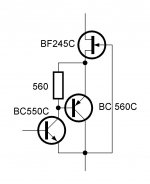
Hi Lazy Cat... i see, do you have any schematic that have this input? I see that Dr. Bora have use this topology for input stage in his design epsilon
http://bas.elitesecurity.org/epsilon-schematic.pdf
Any schematic more?
http://bas.elitesecurity.org/epsilon-schematic.pdf
Any schematic more?
Any schematic more?
This triple is only a building block replacing single BJT to get better performance. Schematics suitable are any one would like to use, it's up to your imagination.

Member
Joined 2009
Paid Member
Hi,
refferring to the schem of #1, the JFETs require to be high Vgs types which the SK170/SJ74 are certainly not.
The BFs may be useable, but I'd prefer the 4391 due to their higher Vds.
Apart from the BFs and the 439x probabely all other suitable parts are long obsolete.
While a depletion mode device is a elegant way to create the CFPs supply it should be noted that there will be no real complementars to the N-JFETs.
You may be able to find devices for a differential SE input, but not for a complementary symmetrical input.
Also the Drain-Source voltage may be too restricted for a high power amplifier (>50W).
It could well be that the JFET itself needs to be cascoded too.
Further on keep Gate leakage in mind.
From app Vds/4 on and high current and high temperature conditions Gate leakage 'explodes' and could lead to a fatal Latch-up of the device.
The DS values for Gate leakage are given for absolutely non-realistic conditions.
For the CFP BJTs standard BC5xx or BC3xx (and their SMD equivalents BC8xx) are very suitable, easy to source and lowcost.
jauu
Calvin
- Status
- This old topic is closed. If you want to reopen this topic, contact a moderator using the "Report Post" button.
- Home
- Amplifiers
- Solid State
- bjt jfet CFP diff input stage