I have seen similar cross-linked input stage among tube schematics, and have decided to try it with transistors. Main idea is to check, whether zero stability at the output will allow no-capacitors load connection.
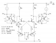
Planned amp schematics is enclosed. At the moment, I have assembled and made some measurements of the input stage only (next simplified schematics).
Some advantages of the cross-linked input stage compared to traditional differential stage - gates of jFETs are almost linked to ground, and they operate almost as cascode stage. PSRR is also good.
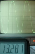
With the voltages indicated, schematics provides 10V RMS undistorted sine, and clipping behaviour is soft.
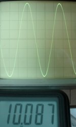
Passband is wide, probably few MHz. Square waves are shown for 1kHz, 100kHz and 1MHz, 15V peak-to-peak.
Zero at the output is adjusted by paralleling some resistor to R5 or R6.
I have found it possible to keep output zero within +- 15mV.


Planned amp schematics is enclosed. At the moment, I have assembled and made some measurements of the input stage only (next simplified schematics).
Some advantages of the cross-linked input stage compared to traditional differential stage - gates of jFETs are almost linked to ground, and they operate almost as cascode stage. PSRR is also good.
With the voltages indicated, schematics provides 10V RMS undistorted sine, and clipping behaviour is soft.
Passband is wide, probably few MHz. Square waves are shown for 1kHz, 100kHz and 1MHz, 15V peak-to-peak.
Zero at the output is adjusted by paralleling some resistor to R5 or R6.
I have found it possible to keep output zero within +- 15mV.
Attachments
Last edited:
Hi Vladimir,
I think you have an error in the schematic drawing, please check it - the Bases of BC177(PNP) transistors are far more positive than their respective Emitters.
I think you have an error in the schematic drawing, please check it - the Bases of BC177(PNP) transistors are far more positive than their respective Emitters.
Last edited:
Hi Vladimir,
I think you have an error in the schematic drawing, please check it - the Bases of BC177(PNP) transistors are far more positive than their respective Emitters.
Juma, no, both bases of BC177 are grounded (the T2 base has some mV positive due to sub-uA base current), and the emitters of T3, T4 are positively biased (0,67V + 0,67V) = 1,35V
This schematics is working correctly.
I should also mention, that measured voltage amplification factor (unbalanced input - balanced output) is close to 10 (in dB it is 20dB). Quite a comfortable value. Output zero instability is even better than I mentioned before, I am observing it for 5 hours now, and it is swinging +- 3mV. But, just after switch-on, it is something like 80mV, and goes down in few minutes. T1...T4 are just Darlington emitter followers, input impedance is rather high.
Last edited:
I think it looks like a very fine design. My only concern, as far as I can see, is that you may have an input offset problem, since you are running the input transistors with about 2 mA and using a 22k resistor?
I think it looks like a very fine design. My only concern, as far as I can see, is that you may have an input offset problem, since you are running the input transistors with about 2 mA and using a 22k resistor?
I use T4 (T3) with hFE=150, and T2 (T1) with hFE=300.
16mA/150 = 0,1mA is the T4 base current
Collector current of T2 is 0,1mA + 0,2mA(R2 resistor) = 0,3mA
Base current of T2 is 0,3mA/300 = 1uA
1uA causes 22mV on the R0 resistor.
At the same time, I agree, that it would be better to deal with balanced input.
Moreover, compared to differential stage, this stage is much more "resistant" to non-symmetric loading.
Last edited:
Yes, for balanced inputs, the problem can be minimized. But have you considered using FETs as input transistors instead of BJTs?
Yes, for balanced inputs, the problem can be minimized. But have you considered using FETs as input transistors instead of BJTs?
One could make a try with input FETs, but the low emitter-base resistance of BJTs provide definite benefits at this schematics, like the "semi-cascode" operation mode.
So you did drift this way,, balanced single ended...🙂 NICE
takes the caps away, why not balance and gain i a transformer..??
takes the caps away, why not balance and gain i a transformer..??
So you did drift this way,, balanced single ended...🙂 NICE
takes the caps away, why not balance and gain i a transformer..??
Caps are not supposed to be used at final version, if output zero drift is OK, than caps will not be needed.
At the moment, caps are used as a temporal protection.
Balanced version is simpy one among possible ways how to prevent passing output signal through power supply.
Trafos are a kind of another "devil", one should avoid caps and trafos if possible. For me, equivalent quality sound is achieved more easy with "proper caps" than with trafos. I have a SE tube amp as a reference, it has both interstage and output SE trafos, designed and manufactured by the most experienced team from Novosibirsk (Russia). I see no problem to get similar sound with caps at the output.
Last edited:
I have used BC177B as input transistors, since I expect they are good at low-currents domain. But they are quite an old-fashioned. Could anybody advise some modern parts, low collector cut-off current bjts, that would be superiour to BC177 ?
Not too fast, but I managed to assemble one complete prototype channel, assembled on the heat sink, and listened to it. I enclose here the as built schematics (also 300pF caps must be added between base-collector of T9, T10 transistors, amp is self-oscillating without them). I also have not shown some caps on the PS rails, driver stage + power rail is separated by 16R-2200u from main + power rail.
Measured output impedance at balanced output is 0,1 Ohms.
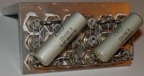
2,7A current sources are assembled with power jFETs (9+9pcs). I like jFET current sources because of two-point connection to schematics. But it of course can be replaced by three-point connected MOSFET or BJT current source.
Sound is close to NoGNFB Ge amp, very vivid.
The heat sink is overrated here, would allow even higher idle current, but I was limited with heating of power supply main trafo (24V + 24V secondaries). Also smaller trafo (12V + 12V secondaries) is used for -9V rail voltage.
I tried to use Ge transistors at the output, but they have been thermally damaged during few seconds after power on, in spite of big heat sink. Dissipation on Ge trasistors must not exceed 20W.
Measured output impedance at balanced output is 0,1 Ohms.
2,7A current sources are assembled with power jFETs (9+9pcs). I like jFET current sources because of two-point connection to schematics. But it of course can be replaced by three-point connected MOSFET or BJT current source.
Sound is close to NoGNFB Ge amp, very vivid.
The heat sink is overrated here, would allow even higher idle current, but I was limited with heating of power supply main trafo (24V + 24V secondaries). Also smaller trafo (12V + 12V secondaries) is used for -9V rail voltage.
I tried to use Ge transistors at the output, but they have been thermally damaged during few seconds after power on, in spite of big heat sink. Dissipation on Ge trasistors must not exceed 20W.
Attachments
Last edited:
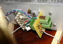
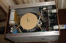
This amp has got its case now, I'll put some pictures later on.
Here is a more detailed schematics, including final power supply filters and input attenuator. I do not have good input pot at the moment for this amp, therefore, as a temporal solution, I've used the 10-position L-pad input attenuator, based on a rotary switch for high-frequency applications with silver plated contacts. It is not so convenient at switching and does not provide wide range of regulation, but quality-wise it is very decent.
Here is a more detailed schematics, including final power supply filters and input attenuator. I do not have good input pot at the moment for this amp, therefore, as a temporal solution, I've used the 10-position L-pad input attenuator, based on a rotary switch for high-frequency applications with silver plated contacts. It is not so convenient at switching and does not provide wide range of regulation, but quality-wise it is very decent.
Attachments

Some impressions about using of rotary switch. One should not use higher resistors values than few kOhms, since silver plated contacts work very good with currents close to a milliamp or some parts of mA. For smaller currents like uA one should look for much more expensive solution, possibly gold over silver followed by palladium over gold plating.
"Balanced NoGNFB With Cross-Linked Input Stage"
If it's balanced by nature, why not having XLR input?
If it's balanced by nature, why not having XLR input?
"Balanced NoGNFB With Cross-Linked Input Stage"
If it's balanced by nature, why not having XLR input?
Yes, XLR input would be more natural and can be easily implemented here.
However, major part of components, that are equipped with balanced interfaces, implement them in an artificial manner, by means of some op-amp following the unbalanced output.
This seems to be a case with my Shanling CD-T1500 player. I prefer its sound from unbalanced output. I have also fine-tuned it by replacing output tubes to selected quard (from ten) Philips Mini-Watt SQ tubes, with excellent final result.
Also, for those who already have RCA high-quality cables, its not easy to pay again for XLR ones.
Speaking about this specific schematics, I used balanced solution mainly with the purpose of excluding an output cap. And, I have got one more confirmation, that NO PS CURRENT CONSUMPTION MODULATION BY OUTPUT SIGNAL is very fundamental principle, allowing higher level of sound quality.
Of course, this principle is not easy to implement at high power amps.
- Status
- Not open for further replies.
- Home
- Amplifiers
- Solid State
- Balanced NoGNFB With Cross-Linked Input Stage