Question about the short circuit protection transistor with current booster in this type of circuit (attached)
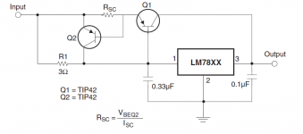
As Iout*Rsc develops enough vbe Q2 to start shunting current away from the base of Q1, does that mean that Q2 only has to handle (at most) the base current of Q1? Or am I missing something here?
As Iout*Rsc develops enough vbe Q2 to start shunting current away from the base of Q1, does that mean that Q2 only has to handle (at most) the base current of Q1? Or am I missing something here?
Attachments
No, I think that Q2 shunts the pass transistor circuitry so you're left with the inherent 78xx short-circuit protection.
Meaning the current short circuit current bypasses R1 and Q1 and goes through Q2 only? So basically max current for Q2 is 78xx @ short circuit?
Yes. Q2 effectively puts an upper limit on the current allowed to pass through Q1.
Yes I see that, cool, but more importantly, it looks like the SC transistor does need to be high power since it needs to pass as much current as the regulator itself at SC. Now I see why in all of the schematics I see both transistors are high power ones.
Short circuit protection doesnt need an additional transistor.
Max current of the regulator is 1A , hence the max voltage through R3
will be 3V , the max voltage across RSC will be 3 - 0.7V = 2.3V so the max current
through the transistor is 2.3/RSC.
All you have to do is to size RSC according to
Max current of the regulator is 1A , hence the max voltage through R3
will be 3V , the max voltage across RSC will be 3 - 0.7V = 2.3V so the max current
through the transistor is 2.3/RSC.
All you have to do is to size RSC according to
- Status
- This old topic is closed. If you want to reopen this topic, contact a moderator using the "Report Post" button.