I told you a bad number earlier: 4 Vp 1 Watt THD 0.00015%
This is not accurate. I did FFT with too little time setting.
Now when I allow FFT to work for a longer time
we get the low and correct value THD 0.00008% for 1 Watt.
The dist at 20kHz is not as pretty, Struth.
But I think it can be low enough ....
The circuit is fast. -3db at 3 MHz, maybe 3.5 MHz
I can't wait until tomorrow when I will try this circuit with BJT output")
This is not accurate. I did FFT with too little time setting.
Now when I allow FFT to work for a longer time
we get the low and correct value THD 0.00008% for 1 Watt.
The dist at 20kHz is not as pretty, Struth.
But I think it can be low enough ....
The circuit is fast. -3db at 3 MHz, maybe 3.5 MHz
I can't wait until tomorrow when I will try this circuit with BJT output
Power Supply +/-42 Volt, 8 Ohm load 4e
THD 1kHz
04 Vp, 01 Watt THD 0.00008%
08 Vp, 04 Watt THD 0.00029%
12 Vp, 09 Watt THD 0.00032%
16 Vp, 16 Watt THD 0.00028%
20 Vp, 25 Watt THD 0.00026%
24 Vp, 36 Watt THD 0.00024%
28 Vp, 49 Watt THD 0.00023%
32 Vp, 64 Watt THD 0.00023%
34 Vp, 72 Watt THD 0.00024%
35 Vp, 76 Watt THD 0.00027%
36 Vp, 81 Watt THD 0.04918%
THD 20kHz
04 Vp, 01 Watt THD 0.00077%
08 Vp, 04 Watt THD 0.00432%
12 Vp, 09 Watt THD 0.00435%
16 Vp, 16 Watt THD 0.00515%
20 Vp, 25 Watt THD 0.00870%
24 Vp, 36 Watt THD 0.01649%
28 Vp, 49 Watt THD 0.03509%
32 Vp, 64 Watt THD 0.07923%
34 Vp, 72 Watt THD 0.21328%
35 Vp, 76 Watt THD 0.38580%
36 Vp, 81 Watt THD 0.66904%
Low Power 1kHz
0.5 Vp THD 0.00006%
1.0 Vp THD 0.00006%
1.5 Vp THD 0.00006%
2.0 Vp THD 0.00006%
3.0 Vp THD 0.00007%
4.0 Vp THD 0.00008% =1 Watt
5.0 Vp THD 0.00010%
6.0 Vp THD 0.00015% =2.25 Watt
7.0 Vp THD 0.00024%
8.0 Vp THD 0.00029% =4 Watt
12 Vp THD 0.00032% =9 Watt
16 Vp THD 0.00028% =16 Watt
20 Vp THD 0.00026% =25 Watt
24 Vp THD 0.00024% =36 Watt
28 Vp THD 0.00023% =49 Watt
Hi Guys
That's very impressive!
The BJTs I use are the MJL3281A/1302A outputs and 2SC4793/2SA1837 drivers - just in case you have similar models in your simulator.... fingers crossed...
I like the idea of the BJTs as their 'lost' supply voltage is a bit less given the lower drive voltage requirement compared to a mosfet. Also, the Vbe threshold is much more predictable than Vgs. I think z-out will be lower with BJTs.
The cost of the MJLs and IRFPs is about the same these days, so cost of one type of output stage versus another does not seem to be an issue, unless you go with 2SK/2SJ outputs that are about three to four times the cost.
Self showed a slightly lower THD with the T-triple output than with the CFP for low levels. That sways me towards the T-type EF output despite the thermal stability of the CFP.
What would really be interesting is the Bryston Quad-complimentary output stage in your buffer format. If you are unfamiliar with this, as a follower output it would be drawn as (for the upper half) an NPN driver with equal-value emitter and collector resistors (typically 33-51R). From the emitter, the base of an NPN output is driven, E to output and C to supply. From the driver collector, a PNP base is driven with C to output and E to supply. This is kind of like a Darlington overlaid with a CFP. The lower circuit half is complimentary to that described.
To compliment the buffer, we need a variable gain discrete gain stage of similar performance. No pressure.
My ideal system would have superlative performance and low noise for listening around 1W and less. A variable gain voltage stage driving a buffer seems like a good way to optimise signal to noise. Why have fixed gain interspersed with attenuations? A buffer that is either pure class-A or has a wide class-A region power and powered from +/-24V or less would suffice.
It would seem possible to overlay a current-monitoring bias servo on your buffer. Either a single Vbe or two across the output device source/emitter Rs with a BJT across the drive lines. Two BJTs in total, either way just holding Vq constant.
Have fun
Kevin O'Connor
londonpower.com
Last edited:
Hi! MiiB, thanks for you reply!in one of "thinkhlin" circuits there was som kind of crosscoupling.. Think that with some work could form some kind of error correction... have you explored that..??
The circuits is No problem for simulation,The solid state has not been completed,I don't how to drow PCB
Hi Guys
Thinkhlin, you should check out Eagle by Cadsoft. They have their version 5 PCB layout software out for a while, up to some level of modification.
I use an older version and lay out lots of boards. It was awkward to learn especially since there was a lot of basic computer stuff I didn't know at the time, but eventually I got there. All these guys with their simulation software will have no problem learning something like Eagle.
Eagle comes with various component libraries, and there are ones users have shared on Cadsoft's site. I made my own parts library as I lay out a lot of tube stuff which do not exist in the stock libraries. Eagle was originally designed around 1984 by computer guys wanting to lay out computer boards. So, there are a few terms used that come from that discipline that might throw off an analog guy at first, but you get used to the idiosyncrasies.
Even if you use only existing parts you will find it convenient to group things you use a lot into a library with a name that puts it at the top of the library list.
Hey Lineup, how about "diamond feedback buffer" for a name, if you do not want your own name on it? This makes sense since a diamond buffer is used as a feedback loop within the buffer. It also answers to the query about adding error correction, as the diamond buffer _is_ correcting the output error.
Have fun
Kevin O'Connor
londonpower.com
Last edited:
For the BJT tryout.Hi Guys
That's very impressive!
The BJTs I use are the MJL3281A/1302A outputs and 2SC4793/2SA1837 drivers - just in case you have similar models in your simulator.... fingers crossed...
I like the idea of the BJTs as their 'lost' supply voltage is a bit less given the lower drive voltage requirement compared to a mosfet. Also, the Vbe threshold is much more predictable than Vgs. I think z-out will be lower with BJTs.
I am using MJL3281A/1302A which have been modeled by ANDY and posted in forum.
I also have the models of 2SC4793/2SA1837, but for my BJT output I will use BD139/BD140 simply. Those are good models which can be found at Home :: NXP Semiconductors
The circuit will use 100mA idle current and the compensation is now 12nF for capacitors.
I will make some figures with the BJT. I be back.
To those not convinced about this circuit I can only say that this is a good thing. And surprised I am that noone has thought about it before me.
To me a very good power buffer is gold worth. It means you can select your own frontend and present it to your loudspeakers with very little distortion. For example use a nice TUBE frontend voltage amplifier and put it to your loudspeaker through the power buffer.
On the contradictionary what is expected the BJT version is more sensitive regarding power supply. When ouput reach above 20 Vp there is an increase in distortion. I can not explain this. Because BJT would be less concerned about voltage supply.
This maybe calls for a cascoding of the current sources and those transistors.
This maybe calls for a cascoding of the current sources and those transistors.
I think a number of people (including me) already have:And surprised I am that noone has thought about it before me.
I have even built a complete one (or attempted to). Actual results are quite promising, but I have already blown an impressive quantity of OP pairs which is a bit tiring, which is why it's on the back burner for the moment.
http://www.diyaudio.com/forums/solid-state/177820-thd-ltspice-3.html#post2377628
Great Elvee.I think a number of people (including me) already have:
I have even built a complete one (or attempted to). Actual results are quite promising, but I have already blown an impressive quantity of OP pairs which is a bit tiring, which is why it's on the back burner for the moment.
http://www.diyaudio.com/forums/solid-state/177820-thd-ltspice-3.html#post2377628
I hope you will get one working good. I see you have had the same thinking as me.
Hi Guys
Elvee, I think your circuit would benefit from using an EF output rather than CFP if only to have more voltage headroom for the error correction circuit to function. This seems to be combined with bias control and it strikes me as a "too clever" solution fraught with disappointment.
Most circuits that have active bias control of some sort would benefit from having a backup clamp circuit. This can be a simple string of diodes across the drive lines. Such an addition seems particularly important in the circuits discussed here that use current sources to turn on the output devices. If the bias control circuit opened, the outputs will be turned on hard and blow themselves up. With a diode clamp in place, maximum current can at least be limited, and hopefully the heat sink is sized to accommodate this fault condition so nothing actually blows up.
The diamond feedback path in Lineup's circuit provides error correction. I believe it to be a unique and new circuit.
The Elvee circuit is incomplete as presented. As a simulated circuit it uses ideal components that are perfectly matched. Emitter Rs will be needed in all positions, to accommodate real-world components. There seems to be no easy way to adjust bias.
To me, it seems like a flaw in most CFB designs that the idle condition in every stage is dependent on that of the input stage. This allows no optimisation for individual stages.
I never use the TO-126 case as it needs too much mounting hardware to go on a heat sink compared to the 2SC4793/2SA1837 which are F-paks. These are the same as the older 2SC3298/2SA1306 that is out of production.
Cordell intrigued everyone with his application of error correction, but the circuit is tweaky. His explanation of how to calibrate it is a bit vague but he does indicate that the benefit of the circuit drops off with frequency, just as all feedback benefits do. Unlike that performance, Lineup's diamond feedback has much less limitation, exhibited by the response to 3.5MHz noted in a previous post.
Have fun
Kevin O'Connor
londonpower.com
Last edited:
Having one robust and reliable enough to be shared as a project on the forum may take some time....Great Elvee.
I hope you will get one working good.
It doesn't really matter: all transistors work with a Vcb>=0. The circuit will absorb transparently anything you care to throw at it: MOS, darlingtons, CFPs: I have even used a quasi.Hi Guys
Elvee, I think your circuit would benefit from using an EF output rather than CFP if only to have more voltage headroom for the error correction circuit to function. This seems to be combined with bias control and it strikes me as a "too clever" solution fraught with disappointment.
Yes, that is exactly what I used at the first stages as an idiot-proof safety net. But it doesn't help for severe oscillation problems that cause cross-conduction, and it has to be removed for actual performance tests because even a small parasitic current degrades the performance: the bases need to be completely independent.Most circuits that have active bias control of some sort would benefit from having a backup clamp circuit. This can be a simple string of diodes across the drive lines
I know...... Such an addition seems particularly important in the circuits discussed here that use current sources to turn on the output devices. If the bias control circuit opened, the outputs will be turned on hard and blow themselves up.
On the contrary, it is quite straightforward: I4 is a little larger than the difference between I1 and I3. The small excess sets the quiescent current: Iq=(26*ln((I1-I3)/(I4-I1+I3)))/R1.The Elvee circuit is incomplete as presented. As a simulated circuit it uses ideal components that are perfectly matched. Emitter Rs will be needed in all positions, to accommodate real-world components. There seems to be no easy way to adjust bias.
This can be done by making I4 (and I6 obviously) adjustable
It doesn't really matter hereTo me, it seems like a flaw in most CFB designs that the idle condition in every stage is dependent on that of the input stage. This allows no optimisation for individual stages.
The small signal bandwidth of this type of circuit is substantial, even with the crap components I love to use. Power bandwidth is obviously more limited.Cordell intrigued everyone with his application of error correction, but the circuit is tweaky. His explanation of how to calibrate it is a bit vague but he does indicate that the benefit of the circuit drops off with frequency, just as all feedback benefits do. Unlike that performance, Lineup's diamond feedback has much less limitation, exhibited by the response to 3.5MHz noted in a previous post.
I see what you mean, ElveeHaving one robust and reliable enough to be shared as a project on the forum may take some time....
Having an idea is one thing.
Making the idea work properly is another cup of tea.
It is lots of work and maybe change some things to make it better.
Here is where the other guys come in. To critises and make suggestions.
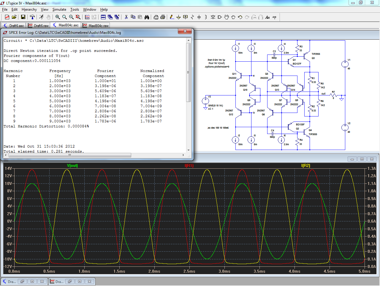
I have now made some numbers from a BJT output.
It works almost as good as MOSFETs.
If I should pick one today it would be with MOSFETs.
Anyway here is the numbers for the BJT 3281A and 1302A output.
Those models are good. Made by Andy_c
And here is the circuit I use for those numbersPower Supply +/-42 Volt, 8 Ohm load 5c
THD 1kHz
04 Vp, 01 Watt THD 0.00009%
08 Vp, 04 Watt THD 0.00012%
12 Vp, 09 Watt THD 0.00017%
16 Vp, 16 Watt THD 0.00022%
20 Vp, 25 Watt THD 0.00029%
24 Vp, 36 Watt THD 0.00037%
28 Vp, 49 Watt THD 0.00052%
32 Vp, 64 Watt THD 0.00962%
34 Vp, 72 Watt THD 0.02946%
35 Vp, 76 Watt THD 0.04130%
36 Vp, 81 Watt THD 0.05396%
Attachments
Maybe you can improve distortion figures by elevating voltage for U3, U9. Add diodes in series with the R14.
dado
Or add another follower gain stage
That circuit is similar to the amplified diode that is the basis of HEC but it is a little different. U3(U9) still act as the differential amplifier where one input is the VAS and the other is the output node. The difference signal becomes the 'error correction' component. HEC utilizes feedback/feedforward instead of just nested feedback. Also the FB/FF loop has near unity gain(high BW) in the HEC amplified diode. What kind of temperature sensing scheme have you come up with? I assume U3(U9) would be mounted with the output transistors.
Hi Guys
The BJT circuit is good as is. Definitely leave out series diodes in the audio path.
But... I think it would benefit from being a triple-EF instead of just a double-EF. This has the benefit of allowing lower front-end currents and a higher input impedance along with the usual benefits. Similarly, paralleled outputs provide a larger class-A region, more constant gm, lower output impedance, reduced stress on the driver, etc.
Elvee, a circuit that is so sensitive to tiny capacitances has more serious problems than you seem to wish to acknowledge. You said yourself that you blew up a lot of output devices. Does your statement that the circuit transparently "accepts" any type of output device really just mean it blows them up in egalitarian fashion? It has been amply demonstrated that circuits requiring finnicky adjustment of precise current/voltage/gain values are not reliable performers in the real world. The circuit form posted here is in that category.
Lineup's circuit has a simpler error correction path and has been fitted with normal add-ons required to build a practical circuit - degeneration resistors, gate-stops, etc. I have a working version here built similarly to the BJT circuit but with a triple instead. For the circuit to be "universal", I think the input impedance needs to be higher than it is now headed and the triple helps with that.
The Lineup THD numbers for 1kHz and 20kHz are already phenomenal - and they started off that way! Kudos to a good design. What really needs to be seen is the distortion profile. The idealised sim will be low for even orders and higher for odd orders. A real circuit won't balance out the evens so well, so the actual distortion profile should be fairly balanced and should sound good.
Lineup, on the first mosfet form, the sim showed that for 44Vpp input, the input current was just over 4mApp. That was with 20mA in the front-end. How do the peak drive currents look for the 40mA input circuit?
Have fun
Kevin O'Connor
londonpower.com
Hi Guys
The BJT circuit is good as is. Definitely leave out series diodes in the audio path.
Then you have to leave out all transistors in the audio path.
dado
Problem is not tiny capacitances or otherwise, but the huge loop gain that gives the circuit its "magical" properties. Real wiring has inductances, resistances, etc and there is an infinite combination of them that can turn the circuit into an oscillator.Elvee, a circuit that is so sensitive to tiny capacitances has more serious problems than you seem to wish to acknowledge.
See above. The one thing it does not require is finnicky adjustment for DC conditions or similar, and it accepts any type of device without readjustment or change in performance.You said yourself that you blew up a lot of output devices. Does your statement that the circuit transparently "accepts" any type of output device really just mean it blows them up in egalitarian fashion? It has been amply demonstrated that circuits requiring finnicky adjustment of precise current/voltage/gain values are not reliable performers in the real world. The circuit form posted here is in that category.
Problem is the stability, both local and when it interacts with the main feedback loop(s).
Simpler and degenerated versions can be made to work, but at the cost of blunted performances, which does not interest me.Lineup's circuit has a simpler error correction path and has been fitted with normal add-ons required to build a practical circuit - degeneration resistors, gate-stops, etc.
Even then, the high gain requires due care and attention: watch out the behavior on capacitive load for instance
Hi Guys
Dadod, take your diodes back to the HEC thread.
Elvee, how much performance do you need? Why focus on 'unattainable' when that seems to also mean 'unbuildable'? Cordell did not add all those Rs and Cs to his error correction circuit just to make it complex, nor did he do it to reduce performance. Those parts are needed if you want to build the circuit in this universe.
The Lineup circuit has great performance - and did so right from the start. The point of interest in its development now, at least to me, is to see its distortion profile. So far, the signal source into the diamond feedback emitters has been ideal, but what about ideal plus a small resistance? Performance when driven by the OPA opamp does not interest me as that device is far from optimal.
As I said above, I believe the higher input impedance of the original version will make DC offset correction easier - which is about the only "defficiency" in the circuit. There are many circuits that require a long development period to go from paper to product, but this circuit is not one of them.
Have fun
Kevin O'Connor
londonpower.com
Last edited:
Hi Guys
I don't see why a LED is used in the bias circuit. Thermal compensation would be better with many of the other bias-reg forms where the diodes are in the base circuit.
For example, Leach found that three diodes undercompensated the output stage in his amps, where four diodes nominally should have overcompensated it but did not, fixing thermal issues builders were having.
Although the performance of the first version Lineup buffer tempts me to use mosfets, I would never use a jfet in a bias circuit. Fortunately, a board can be laid out to accommodate mosfet or BJT outputs, along with driver pairs. Gate protection zeners can be either stuffed or not but should be used for the mosfets.
Have fun
Kevin O'Connor
londonpower.com
- Status
- This old topic is closed. If you want to reopen this topic, contact a moderator using the "Report Post" button.
- Home
- Amplifiers
- Solid State
- New Lineup IDEA - Power Follower/Output stage