Hello
I have been working on the following design for some time now, and after various modifications over time I have settled on the attached schematic. I have built this circuit on three different breadboards from different manufacturers, and with mixing and matching components. There are a few nuances, but the circuit works just fine.
I have subsequently designed a PCB and have tried to assemble it. There have been a few problems, and would like your help and suggestions.
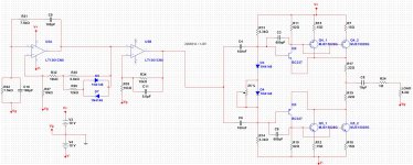
As you can see there is a Wien bridge oscillator at 200KHz and that feeds into a current amplifier in order to drive a load of 8-25R.
My PCB does not have great spans of copper plains, however there are individual ground tracks all leading to a central point. The track widths are adequate for the currents involved.
The first problem is the instability of the Wien bridge oscillator. While it is true that the Wien bridge in general will either clip to the rails or not oscillate at all, the topology I have presented works quite reliably on all three types of breadboard I have tried. However, on the PCB it is almost impossible to stabilise it. As soon as it gets connected to the current amplification stage it produces myriads of much faster oscillations.
This instability has been corrected with the introduction of small feedback capacitor C11 and more importantly with capacitors C3 and C8. On the breadboards I have only used C3 and C8 at 100pF. On the PCB I had to go up to 600pF to tame the unwanted oscillations.
Another problem I have observed is that the introduction of an aluminium sheet under the breadboard, or under the whole of the PCB, with a wire connecting it to the circuit's ground seems to stabilise the oscillator, and the current amplification stage under load.
I have no experience in designing PCB at 200KHz but I am sure normal audio practices would also apply. The beneficial effects of the aluminium sheet under the PCB indicate to me that perhaps I need a lot of ground planes on the PCB, but I am also considering simply mounting the PCB over an aluminium board, since the whole assembly will be inside a plastic box.
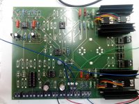
I would appreciate any comments and suggestions on the circuit but most importantly the PCB design. I am also going to attach a photo of the current PCB so you can see the layout of the components so far.
Edit: I have attached a picture of the PCB. I have only assembled the oscillator and current amplification stage so far. There are other parts of the circuit not shown on the schematic.
I have been working on the following design for some time now, and after various modifications over time I have settled on the attached schematic. I have built this circuit on three different breadboards from different manufacturers, and with mixing and matching components. There are a few nuances, but the circuit works just fine.
I have subsequently designed a PCB and have tried to assemble it. There have been a few problems, and would like your help and suggestions.
As you can see there is a Wien bridge oscillator at 200KHz and that feeds into a current amplifier in order to drive a load of 8-25R.
My PCB does not have great spans of copper plains, however there are individual ground tracks all leading to a central point. The track widths are adequate for the currents involved.
The first problem is the instability of the Wien bridge oscillator. While it is true that the Wien bridge in general will either clip to the rails or not oscillate at all, the topology I have presented works quite reliably on all three types of breadboard I have tried. However, on the PCB it is almost impossible to stabilise it. As soon as it gets connected to the current amplification stage it produces myriads of much faster oscillations.
This instability has been corrected with the introduction of small feedback capacitor C11 and more importantly with capacitors C3 and C8. On the breadboards I have only used C3 and C8 at 100pF. On the PCB I had to go up to 600pF to tame the unwanted oscillations.
Another problem I have observed is that the introduction of an aluminium sheet under the breadboard, or under the whole of the PCB, with a wire connecting it to the circuit's ground seems to stabilise the oscillator, and the current amplification stage under load.
I have no experience in designing PCB at 200KHz but I am sure normal audio practices would also apply. The beneficial effects of the aluminium sheet under the PCB indicate to me that perhaps I need a lot of ground planes on the PCB, but I am also considering simply mounting the PCB over an aluminium board, since the whole assembly will be inside a plastic box.
I would appreciate any comments and suggestions on the circuit but most importantly the PCB design. I am also going to attach a photo of the current PCB so you can see the layout of the components so far.
Edit: I have attached a picture of the PCB. I have only assembled the oscillator and current amplification stage so far. There are other parts of the circuit not shown on the schematic.
Attachments
Last edited:
I don't understand why you have complicated with two capacitors (C4 and C6) because I think one capacitor was enough. But fine, let's get over it ...
It's very important here to treat PCBs way, the interaction between your circuit and power supply. Have you thought to conceive and power supply and if so, how? The answer to this question is very important because it can influence, more or less, the design of the PCB.
It's very important here to treat PCBs way, the interaction between your circuit and power supply. Have you thought to conceive and power supply and if so, how? The answer to this question is very important because it can influence, more or less, the design of the PCB.
A picture of the pcb layout, not just a photo, is crucial to enable good suggestions.
It is a two sided PCB, how can I present it here ?
I don't understand why you have complicated with two capacitors (C4 and C6) because I think one capacitor was enough. But fine, let's get over it ...
It's very important here to treat PCBs way, the interaction between your circuit and power supply. Have you thought to conceive and power supply and if so, how? The answer to this question is very important because it can influence, more or less, the design of the PCB.
The second capacitor, on the breadboard has a very small beneficial effect on the amplitude of the wave on full load. On the PCB however it is another story: the second cap seemed to cause millions of harsh oscillations that were only stopped with the addition of C3 and C11 at 600pF (on the breadboard it was 100pF each).
The power supply will be two 12V batteries, but for the time being I am using my bench PSU.
post the gerber files.
Most pcb layout programs allow display / print / export of the copper sides.
Ok here are the gerber files the same ones I sent to the PCB manufacturer. I also attach the full schematic because the one I posted above is not the full thing.
Attachments
Come on!
I cannot display a .sch file. What is that?
You post the wrong schematic with no details of decoupling caps and expect comments on stability?
Please do the work and present the files as .jpg like everyone else!
I can already see from your photo that many components are not fitted to the pcb. How is one to comment intelligently on what is going on?
I'm out.
Come on!
I cannot display a .sch file. What is that?
You post the wrong schematic with no details of decoupling caps and expect comments on stability?
Please do the work and present the files as .jpg like everyone else!
I can already see from your photo that many components are not fitted to the pcb. How is one to comment intelligently on what is going on?
I'm out.
The .sch is a P-CAD ASCII file. I thought it was some kind of standard, but obviously not. I am trying to produce jpeg files of the schematic but it is not easy.
I trust you can view the Gerber files OK?
You probably have a couple of problems.
That can lead to confusion if they interact.
1. It is essential to decouple the power supply to the WB Oscillator section.
Had practical experience with that.")
2. The CFP output that you use is notorious for instability.
If you are not already aware of the issues then there are multiple threads to search. I have just started to study this because fixes seem to be more trial and error than I trust.
Avoid the problem with EF unless you really need CFP.
If so then you can try base stoppers on the outputs, the drivers, between the output collectors and the driver emitters.
Best wishes
David
BTW. Hard to keep everyone happy but many people don't like JPGs either and prefer a lossless format.
That can lead to confusion if they interact.
1. It is essential to decouple the power supply to the WB Oscillator section.
Had practical experience with that.
2. The CFP output that you use is notorious for instability.
If you are not already aware of the issues then there are multiple threads to search. I have just started to study this because fixes seem to be more trial and error than I trust.
Avoid the problem with EF unless you really need CFP.
If so then you can try base stoppers on the outputs, the drivers, between the output collectors and the driver emitters.
Best wishes
David
BTW. Hard to keep everyone happy but many people don't like JPGs either and prefer a lossless format.
Last edited:
In the beginning of this thread I tried to show only the oscillator and the output stage and avoid other parts of the circuit which I have not even built on the PCB and would add confusion. I also could not get a jpeg file output, but now I have done it and am attaching it here.
To summarise in order to stabilise the circuit and eliminate harmonics I have needed to :
a) add big feedback caps to the driver transistors (600pF). These are not shown on the jpeg schematic. On the breadboard model, these were sufficient at 100pF whereas on the PCB I needed 600pF.
b) increase the bias of the output stage until the curve does not suffer from crossover distortion but also until it looks cleaner on the scope - typically 100mA idle. There is no difference here between PCB and breadboard
c) add a zobel of 1R/330nF at the output to eliminate parasitics at the output when the load is a transformer - again no difference between PCB and breadboard
d) add a sheet of aluminium under the PCB and connect this to the circuit "common" - no difference between PCB and breadboard as the breadboard is mounted on an aluminium plate.
e) the wien bridge oscillator on the breadboard is "steady" and not affected by the following stages, scope probes etc. For example I can connect it or disconnect it from the output stage with only a minimal change in waveform. On the PCB however it seems it is sensitive to everything that follows and much harder to control. The 600pF feedback caps have stopped the unwanted oscillations but I am not sure what else is lurking there. I was expecting that the output of U1.2 should be rock steady and imprevious to almost anything that follows short of a short This is true on the breadboard but absolutely not true on the PCB.
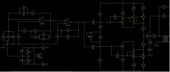
I am thinking that my PCB design is not proper, I have seen other PCBs with huge ground planes on both sides, which is not something I have done (or know how to do). But it may just be something else I have missed. If you cannot see the PCB from the gerber files then I will try to post jpegs of it, even though it is two layered.
Edit: managed to get a better jpeg
To summarise in order to stabilise the circuit and eliminate harmonics I have needed to :
a) add big feedback caps to the driver transistors (600pF). These are not shown on the jpeg schematic. On the breadboard model, these were sufficient at 100pF whereas on the PCB I needed 600pF.
b) increase the bias of the output stage until the curve does not suffer from crossover distortion but also until it looks cleaner on the scope - typically 100mA idle. There is no difference here between PCB and breadboard
c) add a zobel of 1R/330nF at the output to eliminate parasitics at the output when the load is a transformer - again no difference between PCB and breadboard
d) add a sheet of aluminium under the PCB and connect this to the circuit "common" - no difference between PCB and breadboard as the breadboard is mounted on an aluminium plate.
e) the wien bridge oscillator on the breadboard is "steady" and not affected by the following stages, scope probes etc. For example I can connect it or disconnect it from the output stage with only a minimal change in waveform. On the PCB however it seems it is sensitive to everything that follows and much harder to control. The 600pF feedback caps have stopped the unwanted oscillations but I am not sure what else is lurking there. I was expecting that the output of U1.2 should be rock steady and imprevious to almost anything that follows short of a short
This is true on the breadboard but absolutely not true on the PCB.I am thinking that my PCB design is not proper, I have seen other PCBs with huge ground planes on both sides, which is not something I have done (or know how to do). But it may just be something else I have missed. If you cannot see the PCB from the gerber files then I will try to post jpegs of it, even though it is two layered.
Edit: managed to get a better jpeg
Attachments
Last edited:
akis, just open the schematic or view the pc board layers, hit the PrtScr key, open MS Paint, click on edit and then click paste. Save as any format you like.
And would you believe that that is what I do most of the time, except it does not work for Diptrace... I have now done it using "print preview"...
You probably have a couple of problems.
That can lead to confusion if they interact.
1. It is essential to decouple the power supply to the WB Oscillator section.
Had practical experience with that.
2. The CFP output that you use is notorious for instability.
If you are not already aware of the issues then there are multiple threads to search. I have just started to study this because fixes seem to be more trial and error than I trust.
Avoid the problem with EF unless you really need CFP.
If so then you can try base stoppers on the outputs, the drivers, between the output collectors and the driver emitters.
Best wishes
David
BTW. Hard to keep everyone happy but many people don't like JPGs either and prefer a lossless format.
1) I have done that from the start, as you can see from post #12 there are 120R resistors followed by 100uF/100nF caps very close to the op-amp. On the breadboard I can remove completely the resistors and bypass caps and it makes no difference whatsoever to the quality of the output, but I left them in place just in case.
2) I do not understand what is "CFP output" ? What is "EF" ? What is "base stoppers" ?
I do not understand what is "CFP output" ? What is "EF" ? What is "base stoppers" ?
There are 2 common ways to connect the output transistors.
EF = Emitter Follower - The default "standard".
CFP = Complementary Feedback Pair - Some potential benefits but more prone to oscillation. Your circuit is CFP and this is very probably one of your problems.
D. Self and Bob Cordell both discuss these options and provide essential information on the fundamentals. After that there are several, easy to find threads here on CFP stability problems and preventative measures - one of which is a resistor in series with the base, called a[n oscillation] "stopper". Your circuit lacks these so it is not a surprise that it is borderline stable.
Best wishes
David
I created a pcb for a mixer without putting any thought into ground loops.
The pcb came back, I built it up and it hummed like mad. I tried shorting the ground lines with wires but this had limited success.
I redesigned the pcb seperating the audio ground and power supply ground and it worked a treat. There musnt be any power supply currents in the audio ground line so a single point for the grounds to meet is vital.
For class d I found that I needed to keep tracks as short as possible with decoupling as close to the class d chip as possible.
There are 2 common ways to connect the output transistors.
EF = Emitter Follower - The default "standard".
CFP = Complementary Feedback Pair - Some potential benefits but more prone to oscillation. Your circuit is CFP and this is very probably one of your problems.
D. Self and Bob Cordell both discuss these options and provide essential information on the fundamentals. After that there are several, easy to find threads here on CFP stability problems and preventative measures - one of which is a resistor in series with the base, called a[n oscillation] "stopper". Your circuit lacks these so it is not a surprise that it is borderline stable.
Best wishes
David
That is very helpful, thank you. I have done a search and will continue looking out for it.
It's a pleasure. Perhaps it is too late now that you have a PCB but I would recommend the less troublesome EF unless you have a specific requirement for a CFP. That doesn't seem to be the case here.
There is not much detailed analysis of the CFP so if you continue with it and learn any new lessons then be sure to post them.
Best wishes
David
There is not much detailed analysis of the CFP so if you continue with it and learn any new lessons then be sure to post them.
Best wishes
David
Last edited:
I have preferred the compound pair rather than the darlington based on:
1) the darlington has double the voltage drop from the rails. If you are working with batteries then losing 1.2 V from the rails is very significant. With CFP I lose just 600mV.
2) based on Rod Elliot's research the compound pair is much more thermally stable than the darlington pair and he prefers it in all his designs. A link: Elliott Sound Products - Audio Power Amplifier Design Guidelines
So far I have discovered:
I have noticed that the CFP's driver transistor is in common emitter mode, ie it has a resistor on its collector and nothing on the emitter (no feedback resistor), therefore, as seen in isolation from whatever follows, we have a 82R-120R resistor on the collector and a 8R load on the emitter, giving us a voltage gain of 10. Voltage gain usually means trouble, whereas a common collector arrangement should not suffer because there is no voltage gain. So I added the B to C caps to stem any voltage gain at HF, which on my scope looked like 10X-20X the fundamental, ie around 2MHz-4MHz.
On the breadboard there are contact resistances which alter the behaviour of a circuit when large currents pass through (> 50mA). For example I was building a Li-Ion battery charger on breadboard and could not understand the strange voltage readings. It was because large currents of >50mA were causing errors large enough to disturb the rest of the circuit. To get around this problem I identified which component's pins would be passing more than 50mA and soldered two wires on them so that they subsequently connected to the breadboard with two contacts for each one pin. This made things much better, but still not as good as soldered connections.
I also understand that with the CFP this is the same case on breadboard (CFP testing usually means >50mA), so when it comes to HF oscillations the breadboard behaves way differently to the PCB. This must be taken into account.
From the three proposed solutions, ie resistors at bases, resistors at emitters and caps on B to C, I think the latter is the best because you do not lose any voltage from the rails. For example with 82R on the collector and 10R on the emitter as a "HF stopper", you already lose 100mV-200mV - and am not sure if the 10R will stop the HF oscillations at all.
In my case my fundamental frequency is 200KHz, 10 times the audio upper limit, and the 600pF caps have no effect on the output voltage swing, so I suspect that they would also not have any effect on audio frequencies.
I have also found that driving an inductive load (eg a transformer) is very different to driving a resistive load (eg a dummy load resistor). But I added a zobel of 1R/18nF and that stopped oscillations completely.
Biasing is also important, low bias creates HF oscillations when driving a heavy load, you need to increase the bias while under heavy load conditions until the curve looks right on the scope. In my case with +/-8V at the output and a 8R load, I needed about 100mA on "idle" to get a good looking curve at full load.
I have preferred the compound pair rather than the darlington based on:
1) the darlington has double the voltage drop from the rails. If you are working with batteries then losing 1.2 V from the rails is very significant. With CFP I lose just 600mV.
2) based on Rod Elliot's research the compound pair is much more thermally stable than the darlington pair and he prefers it in all his designs.
You trade a major risk of electrical instability for thermal stability improvement that is more theoretical than useful because it is not hard to thermally stabilize an EF anyway.
I have read Rod's articles but it seems an unfavourable trade-off unless you really need the extra 600 mV or have some exceptional case.
Makes some sense for ultra low distortion class A and that's what piqued my own interest.
What's your application? Looks like a Sonar driver or some ultrasonic transducer.
In your case the particular stray capacitances and resistances of the breadboard seemed to have helped to stabilize that layout. Too accidental for my comfort zone, I want a clear analysis, but best of luck.
Best wishes
David
- Status
- This old topic is closed. If you want to reopen this topic, contact a moderator using the "Report Post" button.
- Home
- Amplifiers
- Solid State
- PCB layout problems