PCB rev 4.1
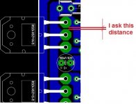
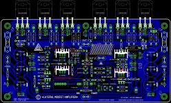
It was a long night , work , but something was created ,PCB rev 4.1 with all in line output transistors . Bensen thanks for hint (good loocking boards too),thanks, also ,for 3 smileys from tinitus .") donpetru , distance it's only0.5 mm , I know too close ,I will change footprint .... As promised PCB rev 4.1 attached
donpetru , distance it's only0.5 mm , I know too close ,I will change footprint .... As promised PCB rev 4.1 attached  Let's see comments , it's not late to make some changes.
Alex.
It was a long night , work , but something was created ,PCB rev 4.1 with all in line output transistors . Bensen thanks for hint (good loocking boards too),thanks, also ,for 3 smileys from tinitus .
donpetru , distance it's only0.5 mm , I know too close ,I will change footprint .... As promised PCB rev 4.1 attached Let's see comments , it's not late to make some changes.Alex.
Attachments
Last edited:
try look at placing power rails and ground from the board middle(connectors at front edge)
might help to try figure power lines and ground like forming a big T, or like a tree with branches
may need jumpers, but would be perfectly ok
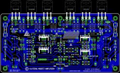
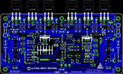
I modified some components in the latest version of the amplifier and used vertical MOSFET transistors. In practice, for reasons of reliability, the number of final power transistors will be higher (three pairs are enough). The results are quite remarkable.
If someone wants, I can make a PCB in the next week and after that is need to do some tests. By the way, which is the user wants to do this tests? Anyone!
I chose this version constructive because parts are easier to find and are cheap.
I do not know if the name DWG amplifier is the best but if you have another idea please let me know. For example, initial "DWG" come from:
Donpetru Wahab Gaborbela
I hope you enjoy this version of the amplifier.
Attachments
Last edited:
If someone wants......QUOTE]
repectfully waiting for Alex to finish his work
I modified some components in the latest version of the amplifier and used vertical MOSFET transistors. In practice, for reasons of reliability, the number of final power transistors will be higher (three pairs are enough). The results are quite remarkable.
Nice to have a low cost variant but beware that THD will be increased
with Hexfets , although it is mainly second harmonic that increase by 6dB.
In your schematic , power dissipation of a VAS branch is reduced
thanks to a 10K resistor , wich is a solution used in many such designs.
The drawback is that at power on the said VAS branch will need
to wait for the supply voltage to reach a higher value before being fully
fonctionnal , that s why i didnt retain this solution.
Rather , a transistor as voltage shifter , as in the mod below ,will be more efficient since it wont limit the VAS current at low voltages.
It was a long night , work , but something was created ,PCB rev 4.1 with all in line output transistors . Bensen thanks for hint (good loocking boards too),thanks, also ,for 3 smileys from tinitus .
Alex.
Great work Alex , this is the most DIY friendly of the lot for mechanical implementation...
A few points that will help in this PCB design and in future ones since
you have skills in this domain.
The Jfets inverting input track is very well done as it s extremely
short , a point that is important for any high feedback amp as this one.
Q7 has lot of room to eventualy use a bigger heatspreader , a good point
since this transistor has the higher dissipation of all TO126.
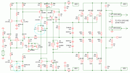
The compensation network is the single most critical part for stability and as such the compensation network from base of Q6 --> C2 --> C3 -->Q8 base must be as short as possible in any amplifier but particularly on those using cascoded VAS where this loop will be active at frequencies exceding 100Mhz.
Whenever other parts of a PCB can have less importance , this one should be designed as a VHF circuit.
In principle any output inductance should be parraleled with a resistor ,
1R in the case of this amp , but i wouldnt recommend putting this network
on PCBs as compacts as this one.
Q9 need no heatsink as it is used as diode and has low VCE , all the dissipation in this branch of the VAS is devoted to Q7 and in fact this transistor is the one that keeps me wondering , so i propose to have its dissipation shared with an added transistor , as is done in nearby designs such as Symassym but with an elegant solution to bias this transistor using the meddle point of the two 33K resistors that bias the zener references and wich is exactly at the desired potential , close to 0V.
Below is the modded schematic. with the additions cercled in blue.
If one choose to not implement the transistor all he has to do is to put a strap between its Collector/Emitter holes.
Attachments
@wahab, I think he forgot ... suppose.Did Wahab also want to do that and forgot to show the ground ?
might help to try figure power lines and ground like forming a big T, or like a tree with branches
may need jumpers, but would be perfectly ok
just a very simple drawing, and my humble suggestion
Attachments
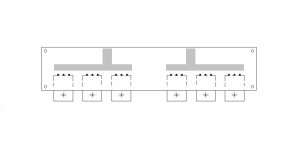
To me it looks like the base of Q20 and the junction of the two resistors connected to it should all go to ground .
Did Wahab also want to do that and forgot to show the ground ?
@wahab, in the last diagram you posted would be better to be connected to GND the base pin Q20 transistor. It's better that way.
I attach in the next few days own version of this amplifier with PCB. It will be a surprise.
Hi Donpetru and Ashok
You are right that connecting the said node to ground seems
at first look logical but i willfully connected it this way since
it allow to get rid of current bias running through the ground
as well as limiting the effect of parasistic capacitance.
If this point is connected to ground then there will be an AC
coupling from emitter and collector to ground through
the device parasistic capacitances.
Indeed , the resistors having same value , the potential is
close to 0V at this node.
Last edited:
I did some tests with and without the transistor Q20 and arrived at the following conclusions:
- If used Q20, then THD value decreases from 0.008% to 0.007% - keeping C12 = 10nF (the capacitor is not critical but after testing it's better 10nF instead of 1nF);
- If we use three pairs of MOS transistors when power dissipation of each transistor (when the amplifier operates in 4 ohms) is only 25W. Seeing this, I simulated the operation amplifier into 2 ohms and in this case each MOS transistor power dissipation is 46W. So, the amplifier can handle quite stable 2 ohm loads. One advantage that you rarely see in other amplifier diagrams.;
- In the last amplifier diagram posted by @wahab we recalculated the value of C13:
C13 = (0.04 * I) / Uz = (0.04 * 0.0025) / 3.6 = 0.27uF
I will choose a standardized value of 0.47uF (once again, value is not critical, but it's better that way);
- C9 and C10 can be 100uF. I noticed enough that;
- In the input circuit will keep my components (I refer to the R1, R2, C2 ...). It's better that way.
- This week I will make my own version of the amplifier PCB with IRFP240/9240, which again, works flawless and is much cheaper than the proposed version of @wahab;
- VAS and input circuits I chose do not supplied with 65VDC because dynamic performance remain the same, so it is pointless. I chose to work all the + /-55VDC that is exactly what amplifier needs.
In the next few days are going to post schematic and PCB amplifier. It will be something special, do not miss the next message for you do not know what losing. It will be a surprise.
Donpetru hardly wait to see your circuit you come up.
wahab
Today I made the laser photocopy for the layout after my design.
I didn't used Q20 because you just came up a few days a go with that idea.
It is worth to implement the Q20 into my layout and go to Staples for laser printing again?
I waited a few weeks and I had that idea it will be no further improvement or other mode on the circuit.
I would like to ahead with these project also.
Guys do you mind if donpetru post his creation here or keep these thread for the Hitachi laterals?
I ask these because once I already ask the moderator (Tinitus) to clean up the mess in these tread... I respect those people interest (opinion) who follow these thread!!! So please vote or just let us know what do you think!
To me is OK but these thread not just about me!
Greetings Gabor
Last edited:
Very nice Alex!! Congrat...
In did these is so nice it would be great to start a GB if it will be enough interest..
I didn't went over to look for any error. I'm just tired to do that because I made several layout with out any software.
Only one question I have
Do we need all those 100uF caps for each mosfet?
Greetings Gabor
Congrat...In did these is so nice it would be great to start a GB if it will be enough interest..
I didn't went over to look for any error. I'm just tired to do that because I made several layout with out any software.
Only one question I have
Do we need all those 100uF caps for each mosfet?
Greetings Gabor
Today I made the laser photocopy for the layout after my design.
I didn't used Q20 because you just came up a few days a go with that idea.
It is worth to implement the Q20 into my layout and go to Staples for laser printing again?
I waited a few weeks and I had that idea it will be no further improvement or other mode on the circuit.
I would like to ahead with these project also.
I m sorry to come late with this modification as it was consequent
to the choice of 2SA1360 instead of the expensive 2SA1407 and
after i compulsed the datasheets more closely.
2SA1360/2SC3423 have only 5W max TDP while using 65V rails will
lead to about 1.2W dissipation for Q7 , quite a lot for a single device so
i elected to use two devices with each one dissipating 0.6W.
As pointed by Donpetru this reduce THD slightly but this is not
the reason that pushed me implementing this mod , it is a question
of long term reliability as my experience is that local hot spots
on a PCB will forcibly induce failures sooner or later.
I did some tests with and without the transistor Q20 and arrived at the following conclusions:
- If used Q20, then THD value decreases from 0.008% to 0.007% - keeping C12 = 10nF (the capacitor is not critical but after testing it's better 10nF instead of 1nF);
In fact anything higher than 100pf is enough , i took 1nF since
this allow using cheap MKP/MKT caps.
- In the last amplifier diagram posted by @wahab we recalculated the value of C13:
C13 = (0.04 * I) / Uz = (0.04 * 0.0025) / 3.6 = 0.27uF
I will choose a standardized value of 0.47uF (once again, value is not critical, but it's better that way);
Not very critical perfs wise but 100nF for both zeners is optimal
for low power on thump , 220nf works as well but higher values
will increase the amp settling time at power on.
- C9 and C10 can be 100uF.
It also works well enough since the amp has basicaly good PSRR.
- VAS and input circuits I chose do not supplied with 65VDC because dynamic performance remain the same, so it is pointless. I chose to work all the + /-55VDC that is exactly what amplifier needs.
Indeed , this increase the long term reliability while perfs are not
affected set apart a slightly lower power but who do listen music
at more than 2 x 100W RMS at home ?.....
- Home
- Amplifiers
- Solid State
- All Hitachi Lateral Fet amplifier for DIY described by Paul Kemble