I would throw away T7 & T8 & T9 and go back to a BJT CCS and a BJT mirror.
if nothing else , using those mosfets for T8 and T9 CCS-es is waste
simple Wilson two bjt CCS for T8 position , mirrored to T9 position, is better solution , freq. wise and dyn. imp. wise
I'm not saying your recommendations are not good but not targeting recommendations to this topic, to create an audio amplifier with only MOSFET and/or JFET transistors.
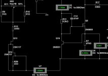
Speaking of the latest version of CCS, not bad to be taken into account next CSS topology. Look at the attached image below.
Attachments
I'm not saying your recommendations are not good but not targeting recommendations to this topic, to create an audio amplifier with only MOSFET and/or JFET transistors.
........
your choice ;that's the same as you said that you want to make entire car wheel from steel
use whatever part , but best for position/role
......
Speaking of the latest version of CCS, not bad to be taken into account next CSS topology. Look at the attached image below.
which one - left (cascoded Jfet , depletion mode biasing ) , or right one (bjt+mosfet,enhanced mode biasing) ?
Your comparison above is totally wrong.your choice ;that's the same as you said that you want to make entire car wheel from steel
use whatever part , but best for position/role
This project it's just a theoretical exercise that would follow a practical approach. Must demonstrate that it can. What will get, remains to be seen.
I mean of both CSS, from the right and left image posted above. Is just one example.which one - left (cascoded Jfet , depletion mode biasing ) , or right one (bjt+mosfet,enhanced mode biasing) ?
Hello
Actually I want to build these amplifier from all fet. Otherwise it will be just another amplifier....
After I test it we can always change to get better performance in case it will be a need.
Yes I want a good (or great) performance IT WOULD no reason to DIY!
For that reason I do not reject any idea specially when a few guys advise the same think!")
Zen Mod
These how you tought to use BJT for T8 & T9?
Please let me know.
Thank you
Greetings Gabor
Actually I want to build these amplifier from all fet. Otherwise it will be just another amplifier....
After I test it we can always change to get better performance in case it will be a need.
Yes I want a good (or great) performance IT WOULD no reason to DIY!
For that reason I do not reject any idea specially when a few guys advise the same think!
Zen Mod
These how you tought to use BJT for T8 & T9?
Please let me know.
Thank you
Greetings Gabor
Attachments
Last edited:
The amplifier can be all fet.
The CCSs are just sources and sinks for the current flows to/from the rails. they can be BJT and the amp is still all fet. At least that's my view.
If you don't afree then use jFETs wired as CCSs. You can add fet cascodes around the jfet CCSs, if you need more voltage capability.
The CCSs are just sources and sinks for the current flows to/from the rails. they can be BJT and the amp is still all fet. At least that's my view.
If you don't afree then use jFETs wired as CCSs. You can add fet cascodes around the jfet CCSs, if you need more voltage capability.
Hello
Actually I want to build these amplifier from all fet. Otherwise it will be just another amplifier....
After I test it we can always change to get better performance in case it will be a need.
Yes I want a good (or great) performance IT WOULD no reason to DIY!
For that reason I do not reject any idea specially when a few guys advise the same think!
Zen Mod
These how you tought to use BJT for T8 & T9?
Please let me know.
Thank you
Greetings Gabor
The collector and the emitter should be inverted in your schematic.
Also , using bipolar would allow to reduce the zener to a few volts ,
extending the maximum voltage swing , although it s doable
with mosfet current source , just take a 5.1V zener and set R3 to 470R ,
while R2 is to be changed to 1.5K.
The original value of 1.8K along with a 15V zener was indeed
not the good set in respect of the original schematic wich
used a 16K resistor to set the input stage current at about 4mA ,
while the combination Z15V/1K8 would have provided 8mA or so.
Anyway , once you have made the choices of components
i will do a few sims to check grossly how this work.
Last edited:
The collector and the emitter should be inverted in your schematic.
Also , using bipolar would allow to reduce the zener to a few volts ,
extending the maximum voltage swing , although it s doable
with mosfet current source , just take a 5.1V zener and set R3 to 470R ,
while R2 is to be changed to 1.5K.
The original value of 1.8K along with a 15V zener was indeed
not the good set in respect of the original schematic wich
used a 16K resistor to set the input stage current at about 4mA ,
while the combination Z15V/1K8 would have provided 8mA or so.
Anyway , once you have made the choices of components
i will do a few sims to check grossly how this work.
Hello wahab
Thank you very much, sim would be great it would save a lot of energy and time. Eaching PC board, soldering etc.
I made those mode you ask for change those parts values, I hope now those BJT-s are OK.
(Usually collector connected to the supp voltage that is why I made that way.)
In case still no good I will re do it again.
Since I don't know those BJT-s drawn correct or not.
Any way I will stick with these Toshiba 2SC3423 transistor we already chose for cascode to.
Thanks one more time!
Greetings Gabor
Attachments
Last edited:
Hello wahab
Thank you very much, sim would be great it would save a lot of energy and time. Eaching PC board, soldering etc.
I made those mode you ask for change those parts values, I hope now those BJT-s are OK.
(Usually collector connected to the supp voltage that is why I made that way.)
In case still no good I will re do it again.
Since I don't know those BJT-s drawn correct or not.
Any way I will stick with these Toshiba 2SC3423 transistor we already chose for cascode to.
Thanks one more time!
Greetings Gabor
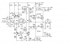
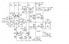
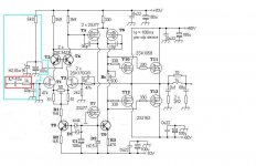
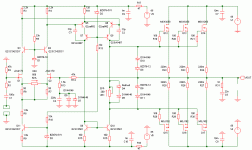
Here a schematic that will summarize the lasts changes.
Some resistors are brought to the closer E12 values ,
such as 1.6K being changed to 1.5K in the input differential
current source collector.
Also , the gain is increased to 33 as the original value , 22 , is too low
for the expected output voltage , it is even likely that it must be
increased even more but it ca be changed later by swapping
the usual resistor.
A diode + led are connected in parralel with the biaising trimmer ,
as this will limit the current if ever the trimmer goes broken
or if it is too much rudly handled , in both case the led will
be bright only with faulty conditions.
The two compensation capacitors are increased to 47pF
to prevent oscillations , they can be later experimentaly reduced
to a lower value.
Attachments
Hello wahab
Thank you very much!
There is something on your change I do not really understand. I did put a bracket on your circuit on those parts..
Also I see you change the total input:
1) Do we not need input capacitor?
2) What about resistor in the input?
I think it has some noise reduction when we use some resistor. I know a many amplifier built with out that resistor.
Please let me know what do you think.
I will apply your new mode to the circuit.
If you can run a sim with these mode it would be great.
Otherwise I just readjust the layout again and again. Of course it is still better than real life test!
Thank you one more time.
Please read donpedru post, do we need to apply the suggested mode. now on your new circuit?
Greetings Gabor
Attachments
Also , the gain is increased to 33 as the original value , 22 , is too low
for the expected output voltage , it is even likely that it must be
increased even more but it ca be changed later by swapping
the usual resistor.
Hello wahab
OK now I start to get it...
1) My two question the input capacitor and a 1K resistor..
2) donpedru mentioned the Rt lower and R3 higher value
After I will redraw the whole circuit .
Thanks one more time.
Greetings Gabor
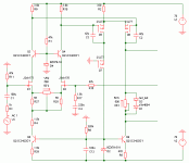
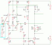
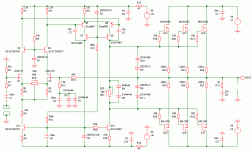
This is the circuit i did use for simulations , the input capacitor and resistance
are inverted compared to your schematic but that doesnt matter for simulations,
the way you did put it on your schematic is correct , though.
1.) It s better to use an input capacitor , just use a value large enough
so the capacitor induced distorsion is reduced to next to nothing.
2.) A 1K resistor in serial with the input should be enough , more
is useless.
The diodes in serial with T8 base are no more needed but it would be
cautious , and i omitted it in the schematic above , to put a 1K resistor
in serial with T9 base.
As for Donpetru proposition to increase R3 , such a mod would reduce
the current through T6 wich would then be unbalanced with the current
that run through T5 , so it s better to stick with the 470R value.
Currently , each of theses transistors should run about 10mA wich
is enough for the VAS to provide adequate slew rate to drive the
output mosfets , less is not desirable.
Also , the 6.8K resistor in your schematic should be increased to 33K at least,
as it s useless to have largely oversized biaising currents that will only
increase thermal dissipation while reducing reliability and without providing
the slightest advantage in perfs.
As for Rt , using a value of 220R would be cautious for the first try ,
it can always be adapted later as the output fets threshold voltage
for a pair at 100mA can be as low as 0.2V and as high as 2V ,
commanding a theorical resistance between 20 and 200R for a current
of 100mA/transistor.
Last edited:
After I will redraw the whole circuit .
To spare you some hassle , wait till complete simulations tell what
exactly can be extracted from this circuit.
So far , the few i already did point to some of the ideas
provided by a few members as being good solutions to have
the best possible perfs without complexe schematic.
Particularly , the VAS is a sensitive part and i d like to see
what is the best solution although given the low gain
of the mosfets it s likely that an all BJT VAS could be
way better for the purpose.
Of course , it wouldnt be no more an all fet amplifier
but it would use them where it matter most , at the input
and at the output , with the BJTs in the meddle...

Particularly , the VAS is a sensitive part and i d like to see
what is the best solution although given the low gain
of the mosfets it s likely that an all BJT VAS could be
way better for the purpose.
Of course , it wouldn't be no more an all fet amplifier
but it would use them where it matter most , at the input
and at the output , with the BJTs in the meddle...
Hello wahab
I agree with that sentence!
You know I want to build it to listening music (a good quality as possible) not for display.
Actually when I listen music I would love to forget the amplifier etc!
If BJT help to get better sound I'll gladly sacrifice the all fet idea.
Quality VS Idea
I think 99.99% would pick the quality.
Just in case if we can achieve a great performance using fet-s let s stick with fet.
When so many experienced DIY-er advise to go with BJT VAS I have to take it seriously.
I'll wait on your sim.
Thanks again
Greetings Gabor
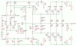
Well , some simulations results.
For information , here the different versions that i simulated ,
1st) is the basic schematic using fets as VAS.
2nd) only swap the VAS fets for BJTs.
3rd) add a full cascode , as there was one but not on the driving
side of the VAS , and it was used only as voltage shifter.
4th) A current mirror is added as VAS load.
Unsurprisily the BJT VAS give better results particularly lower distorsion.
Cascoding the VAS allow to further reduce THD, particularly the second harmonic
that otherwise would be of high amplitude compared to the other distorsion products.
The last modification , adding a current mirror , allow to balance
the VAS current with better precision and lower influence from supply
voltage variations.
Also , it improve the slew rate in the negative going of the signal
and slightly reduce distorsion compared to the third version but both
have THD residuals at 1KHZ below -110dB and below -90dB at 10Khz
at a power of 100W RMS/8 ohms.
I would recommend the two last versions since they are not
more complexe than the original and no more expensive to build.
Some comments from fellow members would be appreciated since
a bunch of brains have forcibly more insight than a single one....
Attachments

Hello Wahab
Thank you for the sim!
I would pick the #3 circuit out of the 4 you posted.
Interestingly nobody comment your sim or the circuit you came up.
May be we went to far from all FET design?
I do not care as long as we can get a great amp.
My questions
Can we drop the 3 pair power mosfet and with that the source resistors?
I don't care if we don't get 100W at 8Ohms.
No need for that extra power.
Thanks one more time
Let s wait if we will get some comment, advise etc.
Greetings Gabor
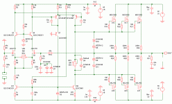
I would pick the #3 circuit out of the 4 you posted.
Good choice since it provide most of the possible perfs...
Interestingly nobody comment your sim or the circuit you came up.
May be we went to far from all FET design?
Can we deduct that it doesnt need any more mods ?.
Can we drop the 3 pair power mosfet and with that the source resistors?
I don't care if we don't get 100W at 8Ohms.
No need for that extra power.
Of course it can be made lower power just by reducing
the supply voltage wich allow to reduce the output stage
components count but this must be done accordingly to the
devices capabilities.
Three pairs are needed for +-55V output stage supply,
Two pairs will suit for +-45V while a single pair , wich i wouldnt
recommend , mandate no more than +-35V and even less if 4 ohms
speakers capability is a requirement , all this assuming that the
front end has +-10 higher supply voltage than the output stage.
The Advantage of a triple pair is that it has lower voltage drop
and allow to use a single PSU voltage for both the output stage
and the front end , hence removing the need of separate rails.
As for removing the source resistors , it is possible if the mosfets
are matched , no need of extremely accurate matching since
the Renesas/Hitachi have some desirable caracteristics that
allow such a direct connection and yield a balanced iddle current.
That wouldnt be possible with Hexfets or with popular Toshiba devices.
Hello
Thanks to wahab for the sim, and he came up a couple version.
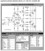
Out of the four I picked these one!
Since I already made several layout and mode it would be great some feedback on the circuit before I do start to work on the layout.
Yes I'll go with 3 pair power mosfet, I have a transformer 40-0-40VAC 750VA or I share the transformer with my Aleph2 2PC 39-0-39VAC 600VA/each.
The transformer I'll use will depend on the bias req. of the amplifier.
I'm not sure what would be the right bias (VA rating of the transformer) I do not want another Class A only the first couple Watt
Also I would live to get some opinion how would you com pare these amp to these symmetrical
These use 52V rail Voltage 400mA bias/channel.. The reason I ask because I have these amplifier (stuffed PC boards) but I read symmetrical has problem when is not matched well the N channel to P channel devices.
Those drivers is impossible to be matched!
Thanks one more time for all of you!
Greetings Gabor
Thanks to wahab for the sim, and he came up a couple version.
Out of the four I picked these one!
Since I already made several layout and mode it would be great some feedback on the circuit before I do start to work on the layout.
Yes I'll go with 3 pair power mosfet, I have a transformer 40-0-40VAC 750VA or I share the transformer with my Aleph2 2PC 39-0-39VAC 600VA/each.
The transformer I'll use will depend on the bias req. of the amplifier.
I'm not sure what would be the right bias (VA rating of the transformer) I do not want another Class A only the first couple Watt
Also I would live to get some opinion how would you com pare these amp to these symmetrical
These use 52V rail Voltage 400mA bias/channel.. The reason I ask because I have these amplifier (stuffed PC boards) but I read symmetrical has problem when is not matched well the N channel to P channel devices.
Those drivers is impossible to be matched!
Thanks one more time for all of you!
Greetings Gabor
Attachments
Last edited:
Since I already made several layout and mode it would be great some feedback on the circuit before I do start to work on the layout.
Making a great amp requires a lot of time. You cannot expect a few minutes or hours of Wahab time to create a great amp, especially when topology or devices are limited in options. I might prefer the Grand Mos than the new amp, assuming that it took a lot of time to design the Grand Mos.
One thing that you may have missed is...
You have liked a darlington CFB amp before. Why not build another CFB, but a better one (because darlingtons have bad reputation anyway). Pay attention to the feedback configuration of the Grand Mos. It is preferable than the LTP. The problem with the FET VAS is only the drive for the output mosfet.
It is possible to create a CFB amp that will stand among the best amps, utilizing the SK214, but it would be complex (will be a mix of BJT-FET) and requires a lot of time and effort.
Why not build another CFB amp, such as the SSA, may be you will like it better than your VFB amps.
- Home
- Amplifiers
- Solid State
- All Hitachi Lateral Fet amplifier for DIY described by Paul Kemble