Before building this amp , a few points that matters if black smoke
is not the goal...
1)The biaising trimmer should be about 500R , as already pointed ,
if you use Renesas/Hitachi laterals wich have low Vth.
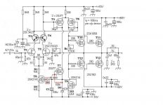
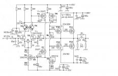
It seems that there is two critical flaws in the schematic.
2) The first is that the VAS current source as well as the differential current
source voltage reference , D2 , is fed by one leg of the differential VAS ,
which is surely a mistake in the schematic.
Second , the differential fet current source has a diode , D1 , in serial with its
gate that is placed the wrong side.
Hello wahab
1) OK I will choose that!
2) Can you help me to correct these mistakes on the circuit (schematic), please..
")
Thank you very much. I do not want to see any black smoke1 Those aren't cheap devices to see a firework..
Greetings gabor
Last edited:
Right. It's an all FET thread !
It would be interesting to see what the comparison between an all FET amp and a mixed device amp will be like.
Hello Ashok
Yes I can replace those after I test the amp!
First and most important to make it work, after we can improve the sound
Thanks for pointing it out.
I already has those mosfets for start!
Greetings Gabor
What is the point of an all-fet amplifier with only a few FETs? It may become optimised from an engineering perspective but the thread becomes meaningless - just another standard design with MOSFETS or HEXFETS for the output stage.
Overall , a BJT VAS works better.
Also , there s no need to use fets for the current sources ,
yet another place where BJTs can be used with much better
predictable behaviour.
Anyway , let s see what can be extracted from an all fet design,
if ever it doesnt suit the expectations changing a few parts
could be done without even changing the layout.
I see now that the last electronic diagram was kept trimmer's of 2K, although I made it clear here:Before building this amp , a few points that matters if black smoke
is not the goal...
The biaising trimmer should be about 500R , as already pointed ,
if you use Renesas/Hitachi laterals wich have low Vth.
http://www.diyaudio.com/forums/soli...mplifier-diy-designed-paul-kemble-naim-5.html
So, if you choose a pair of end 2SK134 / 1057, when Vgs voltage is not the same as with IRFP240 / 9240 and will be changed Rt trimmer value. In fact, if is 2SK transistors, trimmer's value will be less than 2K, in order to avoid accidental adjustment of a high-idle current. The calculation of the value of the trimmer, I expounded on this topic
It seems that there is two critical flaws in the schematic.
1. The first is that the VAS current source as well as the differential current
source voltage reference , D2 , is fed by one leg of the differential VAS ,
wich is surely a mistake in the schematic.
2. ... the differential fet current source has a diode , D1 , in serial with its
gate that is placed the wrong side.
1. It is not a mistake. If you do not understand functioning electronic diagram, then, please...,"stay away".
2. It is not a mistake.
1. It is not a mistake. If you do not understand functioning electronic diagram, then, please...,"stay away".
Providing voltage bias calculations for IRFs while the guy use laterals
without taking a look on datasheets is not exactly a professional path
for whom speaks of "staying away..
I guess that you should use this kind of language with people
in the same range of education as you..
2. It is not a mistake.
It is, for whom has a decent understanding of how this circuit work...
Hello wahab
2) Can you help me to correct these mistakes on the circuit (schematic), please..
Thank you very much. I do not want to see any black smoke1 Those aren't cheap devices to see a firework..
Greetings gabor
I put again the schematic for the purpose.
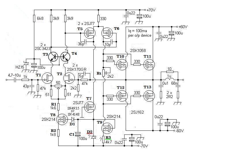
The diode D1 provide the gate biaising of T8 wich is connected
as source follower.
The gate must be biaised positively in respect of the source ,
and as connected it will provide no voltage since the voltage
at the zener is positive in respect of the transistor source.
Hence connection of this diode must be reversed.
Second point , the current through the voltage reference zener D2
is provided by T5 but this transistor current is variable and in case
of saturation it can be switched off to some point , hence there will be
no more a voltage accross the zener leading do disfunctionnent.
Moreover , at power on , T5 will conduct only if T8 conduct but this latter
cant enter conduction if......T5 doesnt conduct!!..
A rapid solution to overcome this second point is to connect a 100K
resistor from zener D2 to ground.
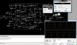
To get over the expression on the language I used above message, I mean the words "stay away". I apologize if you were upset. Look at these two image extracted from a version of the DP400 amplifier. DP400 version posted here is an intermediate version.
In pictures attached below, you will see the idle currents input stage and VAS and performance in dynamic regime of the amplifier.
Of course, how to make CCS is not the best choice but it can provide a performance drop. Indeed, the MOSFET solution in CCS not really thrills me, and when I say this, consider that tell after I built practically and theoretically simulated a lot of audio amplifiers topologies.
Attachments
I see now that the last electronic diagram was kept trimmer's of 2K, although I made it clear here:
http://www.diyaudio.com/forums/soli...mplifier-diy-designed-paul-kemble-naim-5.html
QUOTE]
Hello donpetru
I apologise about that mistake!
I correct it right away.
Thank you for the warning!
Greetings Gabor
The diode D3 in the DP400 schematic can provide a few nA
reverse current wich is enough for fets bias but this
allow the zener to sink an eventual drain/gate excess current
leading to hasardous current source current value that would become
device and Vgd dependant.
All in all , i dont think that it s a good design practice.
A best solution is to put two diodes in parralel , reverse connected,
or better , no diode at all....
Last edited:
wahab; The diode D1 provide the gate biaising of T8 wich is connected as source follower. The gate must be biaised positively in respect of the source said:Hello wahab
Thank you very much. Now is much more understandable to me your advise!
When you gave me some details like how you did in the previous post much better than just write these or that is bad.
Now I can see why do you think is bad!
Thank you very much.
I read many of your post on the forum and I have all my respect to you and everyone who come here with a positive advise!
I didn't purchased the parts (resistors, diodes) yet and I only each one PC board for test purpose.
I would like to keep the circuit as all mosfet (accept cascose)amplifier but in case if we can improve the sound later we can think about to use BJT some place!
At first let s see what we can achieved how is it.
If I would revers the diode how you suggest sill I would need the 100K resistor?
If is not a big request please draw the circuit how you like it with red or any other color so I can print it out! In these case we can avoid confusion to those people who follow the thread.
Otherwise always I have to go back and reread and reread all the posts.
Greetings Gabor
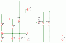
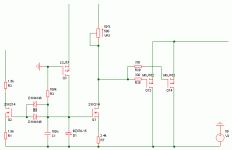
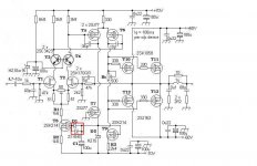
Here is the corrected circuit how donpedru advised a couple days a go!
Attachments
Last edited:
Hello
So D1 is OK how you advised.
D2 I can leave it out you say.
Now these is important because there is a major mod I have to adjust the layout after that.
In these case I can keep how it is.
Thank you very much.
So these circuit is after wahab advise!
Greetings Gabor
So D1 is OK how you advised.
D2 I can leave it out you say.
Now these is important because there is a major mod I have to adjust the layout after that.
In these case I can keep how it is.
Thank you very much.
So these circuit is after wahab advise!
Greetings Gabor
Attachments
What is the purpose of the external zener D1, the 2SK214 has built in gate protection.Suppressing the zener would have nefarious consequences ,
so a few pictures will tell more than a thousand words...
Either one of these two variations below will be adequate...
Last edited:
What is the purpose of the external D1, the 2SK214 has built in gate protection.
That s a voltage reference for the differential and VAS current sources,
not for protection purpose.
In this schematic it will withstand the full half VAS current ,
so it should be a 1 to 2W component , it would be better
to use a lower voltage and set the fet sources resistors
accordingly.
Edit : i thought you were talking of the zener.
As for the diode in serial with the gate , well , i m
still in the expectation about the reason why it was
connected in such a way in the first iteration.
Last edited:
- Home
- Amplifiers
- Solid State
- All Hitachi Lateral Fet amplifier for DIY described by Paul Kemble