Had a look at the files from the link you posted and could not find any simulations of IMD for the F5, only THD.
And the distortion spectra from the F5 simulation dont look like those NP measured with an AP.
Amps that have high THD will have high IMD as well...
The Nelson Pass THD measurements you re talking about
are made at 1W RMS output power....

At least they are measurements. Estimating IMD from a THD simulation that does not match
reality makes no sense to me.
What is senseless is that you dont understand that i simulated THD
at about 6W RMS while nelson pass did measurements at 1W
(for an amp that basically dissipate 100W/channel..
)....Anyway i also simulated IMD ratios for this amp and they are quite high.
Of course , i dont simulate at 1W level , as as such low levels almost
any amp will appear as good enough and Nelson Pass knows it...
Attachments
Last edited:
What is senseless is that you dont understand...
wahab, please refrain from telling me what I understand and what not, OK ?
I have yet to see if real world measurements match your simulations.
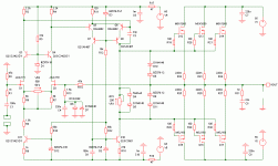
There s a little mistake on the final schematic post 99.
R10 and R12 are marked 100K while they should be 33K each.
I re edited the schematic with the correct values.
Hello wahab
Thank you, I did corrected!
I have some question about the following capacitors.
C9 & C10 is 1 000uF?
C7 & C8 is 10 000uF? I need to know because the size of the capacitor on the layout.
Do the amplifier can be fully driven from a CD player or will need a preamp?
Please let me know
Thank you very much!
Greetings Gabor
wahab, please refrain from telling me what I understand and what not, OK ?
I have yet to see if real world measurements match your simulations.
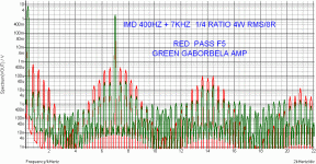
Although the measurements say that it has about 0.1% THD
at 1Khz /20W (not good enough for CD standard) Nelson Pass
specifies it at 1% THD/25W....
http://sportsbil.com/other/NELSON PASS 5 WATT AMP.pdf
Besides , this amp has low gain as he used as much as possible
of it to increase NFB resulting in a meager 15dB voltage gain.
Reducing the gain of the amp discussed in this thread ( wich
is about 30dB) to the same value , would reduce its distorsions by 15dB ,
i let you imagine what would the difference become compared with the F5
in the graph above...
I have some question about the following capacitors.
C9 & C10 is 1 000uF?
Yes , they can be mounted in a separate PCB but in this case put a pair
of 220uF on the amp PCB for wires decoupling.
C7 & C8 is 10 000uF? I need to know because the size of the capacitor on the layout.
This is in fact the power supply minimal caps , on the amp PCB 220uF are enough.
Do the amplifier can be fully driven from a CD player or will need a preamp?
It has a gain of 30 so it can be driven by almost any CD player ,
if necessary the gain can be increased without substancialy altering
the global perfs just by swapping the relevant resistance , R13
in the schematic below.
On another note , hope that your artwork is still in the doing
as it would be valuable to slightly mod the differential and VAS
current sources voltage references in a way that at powering on
the input stage and upper side of the VAS become functionnal
before the VAS current source start to conduct.
This way , the negative feedback will be available micro seconds
or so after the amp is powered on and any eventual pop will be
suppressed or at least reduced to a meaningless amplitude.
Also , it appeared that one of the 33pF compensation capacitor
of the VAS was simply useless , it can be suppressed.
For the remaining 33pF compensation capacitor , it must be connected
with a distance as short as possible from the base of Q6 to Q8 collector.
Also , the track joining Q6 collector to Q8 emitter must be short as well.
On the components side , the transistors used are among the most adequate
for the intended purpose but if they are either too expensive or too difficult
to find there are other models that can be used , just let me know about it
and i ll provide a list of valuable replacements.
I put the updated schematic below , sorry for the late mods, but happily
it is the last ones.
Attachments
Yes , they can be mounted in a separate PCB but in this case put a pair
of 220uF on the amp PCB for wires decoupling.
This is in fact the power supply minimal caps , on the amp PCB 220uF are enough.
It has a gain of 30 so it can be driven by almost any CD player ,
if necessary the gain can be increased without substancialy altering
the global perfs just by swapping the relevant resistance , R13
in the schematic below.
On another note , hope that your artwork is still in the doing
as it would be valuable to slightly mod the differential and VAS
current sources voltage references in a way that at powering on
the input stage and upper side of the VAS become functionnal
before the VAS current source start to conduct.
This way , the negative feedback will be available micro seconds
or so after the amp is powered on and any eventual pop will be
suppressed or at least reduced to a meaningless amplitude.
Also , it appeared that one of the 33pF compensation capacitor
of the VAS was simply useless , it can be suppressed.
For the remaining 33pF compensation capacitor , it must be connected
with a distance as short as possible from the base of Q6 to Q8 collector.
Also , the track joining Q6 collector to Q8 emitter must be short as well.
On the components side , the transistors used are among the most adequate
for the intended purpose but if they are either too expensive or too difficult
to find there are other models that can be used , just let me know about it
and i ll provide a list of valuable replacements.
I put the updated schematic below , sorry for the late mods, but happily
it is the last ones.
You can do some more improvements.
1. increment LTP tail current as jfet vorks bettter close to the Idss.
2. use floating cascode for the LTP, look at attachment.
3. Use Hawksford enhaced cascode for VAS.
4. You do not need to have the same impedance at the jfet LTP input and FB, you can use much smaller resistor for the FB and could do without capacitor.
dado
Attachments
This is interesting, first many claim that simulations results make THD look better than possible real world results.
GK7 youre claiming it makes a good amp look bad.
Btw Wahab is correct, High THD means high IMD. F5 doesnt have low distortion figures but tube amps have even higher and are loved by many although it doesnt mean that they reproduce sound accuratly. Many prefer music with sound effects which is what these high distortion amps do, including F5.
F5 is probably the worst amp I ever played through my BW 804s, even a secondhand 30 euro cheapie rotel sounds better especially with regards to bass. It is not everyones cup of coffee nor does it match many types of speakers.
from post128
Is it about getting the NFB circuit up and working first?
C6 achieve the VAS CCS delay?
is this why some amps start up nearly silently and others cause a varying DC to be exported to the speaker?slightly mod the differential and VAS
current sources voltage references in a way that at powering on
the input stage and upper side of the VAS become functional
before the VAS current source start to conduct.
This way , the negative feedback will be available micro seconds
or so after the amp is powered on and any eventual pop will be
suppressed or at least reduced to a meaningless amplitude.
Is it about getting the NFB circuit up and working first?
C6 achieve the VAS CCS delay?
Last edited:
You can do some more improvements.
1. increment LTP tail current as jfet vorks bettter close to the Idss.
2. use floating cascode for the LTP, look at attachment.
3. Use Hawksford enhaced cascode for VAS.
4. You do not need to have the same impedance at the jfet LTP input and FB, you can use much smaller resistor for the FB and could do without capacitor.
dado
I simulated all theses possibilities , apart from 4 and results are that :
1) Increasing tail current will not improve the perfs , it will just
increase the thermals.
2) A floating cascode is no better be it in AC perfs or PSRR
quite the contrary.
3) An Hawksford cascode will bring no improvement.
4) Using smaller resistors is not a good idea , as if ever
there s a DC output fault there could be enough voltage/current
to break the inverting input fet.
Anyway , thank you for the propositions..
from post128is this why some amps start up nearly silently and others cause a varying DC to be exported to the speaker?
Is it about getting the NFB circuit up and working first?
C6 achieve the VAS CCS delay?
Of course , the usual delayed speaker protection relay
will generaly keep the amp mum but a safe design will always
take care of the standing currents settling at power on
by reducing as much as possible the time necessary for the amp
to achieve stable operation and thus reducing the spike to negligible
time/energy while eliminating all risks of destructive transients currents/voltages within the circuitry.
The case of this thread amp is particularly telling.
In the original schematic the voltage reference is common
for both the differential and VAS current sources.
It can be easily deducted that at power on the VAS current source
will start to conduct before the differential current source can supply
even half of the LTP current so the differential is not functionnal
while the VAS current source has already started to swing the output
mosfet gates to the full negative rail voltage.
This was allegedly corrected by feeding the zener reference with
the second leg of the VAS , hence , the VAS current source could
not conduct at power on since the LTP being not functionnal the second
VAS leg couldnt feed it....but then , the circuit couldnt start at all because
of this chain dependancy :
LTP not functionnal --> VAS non functionnal----->VAS cant supply
the LTP CCS voltage ref.------>LTP non functionnal......
I then proposed to force the voltage ref at power on with a 100K
helping resistor but because of the common voltage ref the VAS
CCS was to kick in first , an undesirable by product , hence the
necessity of separate references.
In the original schematic C6 did extend the time between
VAS CCS starting to conduct and LTP being functionnal hence
increasing the spike energy but in this revised version
the capacitor C6 will effectively act as a further delay for the
VAS CCS conduction , wich is a welcomed effect , but its true role
is to short the AC variations of the second VAS leg ,
otherwise the VAS reference voltage would be very slightly
modulated by the VAS current.
Dadod,
looks like you will have to build the prototype in 5 varieties and prove each of your assertions.
Wahab is not willing to accept without proof.
Oooh it's up to him.
Hello
Thank you for all of you for the reply.
wahab I plan to use serious separate PS, I'm not after to use large 10 000uF-s on the PC board.
When that large caps start to charge up you all know what happen.
If I get the right transformer I will go with reg front end PS.
Small thump not a problem while the capacitors charged but I did notice your advise and I'll take care of that, thank you for the advise!
Guys please do not say the F5 so bad, I want to build the T1 version.
I collected all the expensive parts, heatsink, transformer, Toshiba power devices etc.
All do to me the Aleph30 was a huge upset (because the money energy I invested it didn't showed up), after 45 hours break in I took the boards out from the enclosure and sold them.
I used BG NP caps on the boards, RPR resistors, exotic caps in the PS large Plitron toroid......... close to $$$$ parts value when I count everything including the heatsink, WBT silver solder, connectors etc I do not talk here about the work I invested.
Probably I didn't gave enough time for break in???!!
That is the reason I will (re)build (give another chance to the Aleph) a similar amp Aleph2.
I read many people still prefer the Aleph series over some of the F Watt.
Greetings Gabor
Last edited:
Wahab presented a schematic.
You made 4 suggestions for improvements.
Wahab claims your "improvements" are not such.
Who should prove what?
I just suggested, and wahab said he tried it before, so I am good at it, it is his amp.
dado
I just suggested, and wahab said he tried it before, so I am good at it, it is his amp.
dado
Suggestions were good but they will work for dedicated designs
that will take advantages of such circuits, one must not implement
a sub circuit because it has the reputation to perform well ,
rather a careful examinantions of how this better performances
are provided by a circuit will tell if it s necessary or not to
implement it.
As an exemple the Hawksford cascode can be thought as being
a possible improvement since it does generaly do better because
the common base voltage reference is enclosed in the local feedback
loop but that works only for single ended cascode not for a
cascoded differential as the differential emitters common point
is a virtual AC ground , there will be no AC variations across the common
emitter resistor contrary to the single ended cascode that will see
AC variations through the resistance that load the emitter , while
a differential VAS emitter resistor will see constant current , hence
the Hawksford cascode will not bring any improvement for this kind
of VAS.
- Home
- Amplifiers
- Solid State
- All Hitachi Lateral Fet amplifier for DIY described by Paul Kemble