Hello
Sorry guys I was out for a couple weeks. Now I feel better so back to the project.
I'm looking to get the right transfer paper (from Staples) because I run out of them.
After I will do the PC boards and I will start test the amp. I think I will order PRP resistors that is a great match to the Hitachi laterals..
Thanks for your patient.
Greetings Gabor
Hello
Sorry guys I was out for a couple weeks. Now I feel better so back to the project.
I'm looking to get the right transfer paper (from Staples) because I run out of them.
After I will do the PC boards and I will start test the amp. I think I will order PRP resistors that is a great match to the Hitachi laterals..
Thanks for your patient.
Greetings Gabor
Hi Gabor ,
Hope all is well for you.
As for special resistors , just take regular non inductive ones ,
expensive parts are useless by the way , most of the perfs
are active components dependents.
..... another kind of PCBacording to schematic from post #194
Regards Alex.
Nice board , Alex.
Nice job, Mr. Alex.
Please.... SCHEMATIC WAHAB or SCHEMATIC GABOR?
Thanks!
It is on post 194 but neverless here it is again.
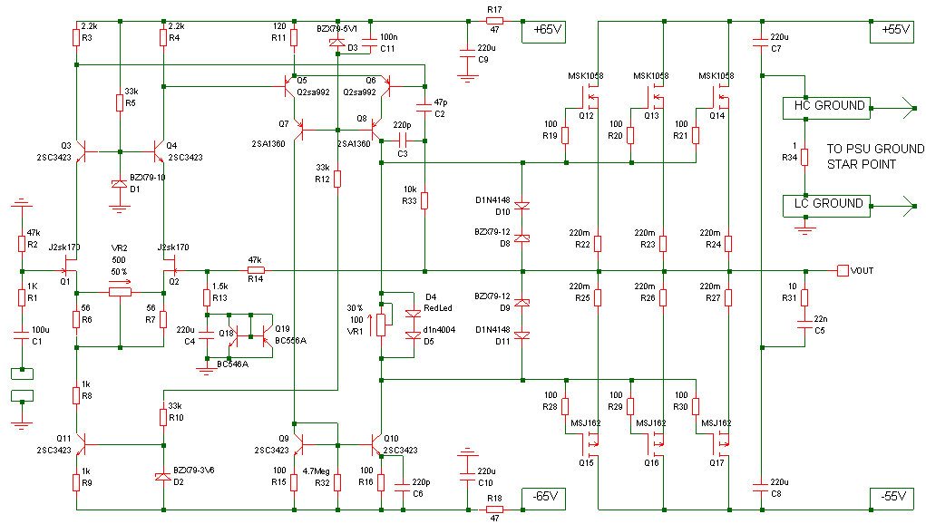
Is C6 across R16 for stability ? Should introduce a zero in the OL gain?
Yes , it slightly extend the unity gain frequency from 15.5Mhz to 18Mhz
but the most valuable change is efficient reduction of the phase lag
at thoses frequencies.
And R33 (10K) does go to the output node and not to the + supply rail ?
You can see that R33 is an AC coupling only , from power output to the inverting input of the VAS to create a local feedback loop that act only at audio frequencies and wich is quite efficient in output stage THD reduction as extensively explained by Edmond Stuart in his insightfull threads about TMC , wich is exactly the role of the compensation capacitors arrangement C3/C2 and R33.
edit : If R33 is connected either to ground or + supply rail the compensation scheme
would be switched from TMC to TPC.
Last edited:
It is on post 194 but neverless here it is again.
Sorry for not being clear.
I meant: Alex wrote on the PCB the words SCHEMATIC WAHAB. I am asking if this schematic comes from you or from Gabor.
Thank you!
.............. If R33 is connected either to ground or + supply rail the compensation scheme would be switched from TMC to TPC.....
Yes that was what I was getting to.
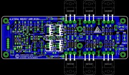
Im sure its electrically perfect, but I still cant help thinking how it would look if the lower fets were 'folded' up in line with their mates
hey, btw, I suppose it would be possible to just omit mounting one output pair if you only want it with two output pair, and maybe lower voltage a bit
hey, btw, I suppose it would be possible to just omit mounting one output pair if you only want it with two output pair, and maybe lower voltage a bit
Hello
Nice design Alex as always, thank you.
Tinitus you right, at these aranjament you need to use some copper heat spreader under the mosfets that would help a lot.
Since all 6 mosfet biased min. 100mA/each and they are close to each other that would be the best solution.
I think we could use these PC board.
Greetings Gabor
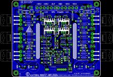
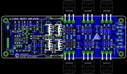
@alex mm, which is the distance between the edge of the pads 2SK1058 / 2SJ162 power transistors ? I think that distance is too small. It's a mistake that is seen in many PCB's that you created. And not only there.
And GND route drawn circular is not a good choice.
By the way, who is the last diagram the amplifier ? I ask this because at one point I gave up watching this topic, which initially wanted something and got something else.
And GND route drawn circular is not a good choice.
By the way, who is the last diagram the amplifier ? I ask this because at one point I gave up watching this topic, which initially wanted something and got something else.
Hello donpedru
All the design work was done by wahab. By the way welcome back.
I know it became another amp how we planed but if you take a look at the sim result it isn't just another amp.
I'd rather gave up my idea to get a nice & a great sounding amplifier!
I'm very happy how it came out! Soon I will fabricate the PC boards and stat testing her.
Alex really nice work! I like it a loot, I didn't took the time to go over but at the first sight very nice!
Alex please do not forget P Danie PC boards design. I had the A30 , those mosfet were very close, biased in full Class A and still worked properly. I used a heat spreader because my heatsink was not one full piece.
I think and believe these will work. We can rotate these PC board if there is a need!!!
Greetings Gabor
looks good, but still ineffective heatspread
heat goes upwards on heatsink
and lower outputs will put heat strain on the upper outputs
please please, put all outputs in one straight line
imagine a 300mm heatsink
board length of 150-200mm seems ideal
well, maybe only in theory
and in reality, after a while they all just get bloddy hot
heat goes upwards on heatsink
and lower outputs will put heat strain on the upper outputs
please please, put all outputs in one straight line
imagine a 300mm heatsink
board length of 150-200mm seems ideal
well, maybe only in theory
and in reality, after a while they all just get bloddy hot
@donpetru distance it's 1 inch ,or 25.4 mm from center to center OT.....
I layout, in few hours, and have joint ground plains , left side with right side yes I admit my mistake , corrected .
Regards Alex.
L.E. I will try tomorow to layout all in line , but for today it's enough .
I layout, in few hours, and have joint ground plains , left side with right side
yes I admit my mistake , corrected . Regards Alex.
L.E. I will try tomorow to layout all in line , but for today it's enough .
Attachments

Last edited:
L.E. I will try tomorow to layout all in line , but for today it's enough .
you get 3 smileys for that try look at placing power rails and ground from the board middle(connectors at front edge)
and perfectly ok to use a wire jumper, when it makes sense to do that
Just an idea for Alex his PCB layout. I used the same position for the OPS in my last amp.
I use 1.5mm² copper wire on the outside of PCB's to solder the output devices on to, when the PCB and OP devices are first mounted to the heatsink. Makes life a lot easier when disassembling the board to make an update or whatever you want to do.
I use 1.5mm² copper wire on the outside of PCB's to solder the output devices on to, when the PCB and OP devices are first mounted to the heatsink. Makes life a lot easier when disassembling the board to make an update or whatever you want to do.
Attachments
- Home
- Amplifiers
- Solid State
- All Hitachi Lateral Fet amplifier for DIY described by Paul Kemble