If you connect your meter to measure the offset and then touch any of the four input transistors with a finger to heat it you will see the offset change. Depending which transistor you choose will determine if the change is higher or lower... try it")
Understood... They have a shroud with heat sink compound
To ensure constant ambient temps... They have been reinstalled
With this on for your info... The 1016s & 2362s arrived sequentially on
Ammo tape so they are consistent BUT I have to check
that the 1016s
& 2362 have same gain code......
Stay tuned
Thanks,
I wouldn't worry over it too much tbh (certainly not at this stage). And do check the other channel too for interest. If you feel it is a problem then you could look at getting "off the shelf" unmatched devices and matching them yourself.
That's me done for tonight. Any questions... just ask
That's me done for tonight. Any questions... just ask
I wouldn't worry over it too much tbh (certainly not at this stage). And do check the other channel too for interest. If you feel it is a problem then you could look at getting "off the shelf" unmatched devices and matching them yourself.
That's me done for tonight. Any questions... just ask
Thanks Mooly .... Will keep this in mind ... Transistor matching that is...for future undertaking.... Once I get the amp to an usable state...
Stay tuned for tonight's finale ... Will be home in 2-3 hours to do the final test...
Must remember to take out 4 amp rail fuses and add 6 amp prior to removing
bulb in AC line ... I didn't want to waste the 6 amp units as I had
a bunch for 4 amp units I was prepared to sacrifice
Stay tuned
Stay tuned for tonight's finale ... Will be home in 2-3 hours to do the final test...
Stay tuned
Couldn't get to it last night..... will perform the final test(s) tonight...
Stay tuned....
Stay tuned....
We're all tuned in... just take it slow and check along the way. No rush
Amplifier is Functional NOW!
Hi Guys:
I connected it up without bulb in AC Line and adjusted the bias accordingly.
I noted the 195mV DC offset and decided to power down and match the 1016's & 2362's in the Differential Input with hfe matched to within <10% between the 1016 pair & 2362 pair (& <5% between the 1016/1016 & 2362/2362).
I got the DC offset down to 80mV on the repaired channel versus <10mV on the good channel.
I ran it unloaded for 2 hours and noted the Bias stayed at 7.0mV +/-0.20mV
and the DC offset stayed constant at 80mV +/-1mV.
So for now I will leave it as is and hook it up to an old pair of speakers to let it run for awhile. I will stick a 100uF VDC EE Bipolar cap in series with the speakers, just in case it lets go in this testing mode. I will do that tomorrow once I get home from work.
I am assuming there is something is still not perfect with the repaired channel, but I assume 80mV is not really a problem as it would be less than 0.0016W of DC @ 4ohms
Let me know what you think.
Thanks in advance,
We're all tuned in... just take it slow and check along the way. No rush
Hi Guys:
I connected it up without bulb in AC Line and adjusted the bias accordingly.
I noted the 195mV DC offset and decided to power down and match the 1016's & 2362's in the Differential Input with hfe matched to within <10% between the 1016 pair & 2362 pair (& <5% between the 1016/1016 & 2362/2362).
I got the DC offset down to 80mV on the repaired channel versus <10mV on the good channel.
I ran it unloaded for 2 hours and noted the Bias stayed at 7.0mV +/-0.20mV
and the DC offset stayed constant at 80mV +/-1mV.
So for now I will leave it as is and hook it up to an old pair of speakers to let it run for awhile. I will stick a 100uF VDC EE Bipolar cap in series with the speakers, just in case it lets go in this testing mode. I will do that tomorrow once I get home from work.
I am assuming there is something is still not perfect with the repaired channel, but I assume 80mV is not really a problem as it would be less than 0.0016W of DC @ 4ohms
Let me know what you think.
Thanks in advance,
Way to go! But I agree with you that maybe the repair is not entirely finished yet, 80 mV is not good enough, especially in light of the good channel's <10 mV.
I wonder what had caused the offset in the first place. Seems that we were mostly chasing a bad replacement part in this thread, that may have diverted our attention from the original cause a bit.
A few questions I have for putting together the puzzle:
Did you keep al failed and/or replaced components? If so, can you mark in the schematic which components failed (and how, i.e. failed open or short)?
Can you do comparative measurements again between the channels?
That's brilliant
Now this 'ere offset. You haven't a fault, just an imbalance due to non matched input devices. It will never be a problem and will never cause a problem.
So that said, how do we improve on it if we want to. Well I notice that Q615 and Q611 are the same type. So next question... can we use these ? And you have two more in the other channel. So you see where this is going
It is only the balance between each of the input stage NPN's or PNP's that matter. You don't have to match NPN and PNP which is impossible anyway despite what you hear about "matched pairs". So if Q615 and the one in the other channel are the same and also Q611 and its opposite number then we have a solution
Q615 and 611 are not critical as they are used as current sources and can be swapped about as necessary or substituted with another device altogether.
Way to go! But I agree with you that maybe the repair is not entirely finished yet, 80 mV is not good enough, especially in light of the good channel's <10 mV.
I wonder what had caused the offset in the first place. Seems that we were mostly chasing a bad replacement part in this thread, that may have diverted our attention from the original cause a bit.
A few questions I have for putting together the puzzle:
Did you keep al failed and/or replaced components? If so, can you mark in the schematic which components failed (and how, i.e. failed open or short)?
Can you do comparative measurements again between the channels?
Hi Jitter:
I believe the "problem" (not really a big issue) is the matching as I notice thet the PNP's (1016's) were matched within 1% (hfe=234/235) and the NPN's were 15% different (236/273).
So I hope Mooly can simulate using his simulatation software.
I will add another post to Mooly's posting
That's brilliant
Now this 'ere offset. You haven't a fault, just an imbalance due to non matched input devices. It will never be a problem and will never cause a problem.
So that said, how do we improve on it if we want to. Well I notice that Q615 and Q611 are the same type. So next question... can we use these ? And you have two more in the other channel. So you see where this is going
It is only the balance between each of the input stage NPN's or PNP's that matter. You don't have to match NPN and PNP which is impossible anyway despite what you hear about "matched pairs". So if Q615 and the one in the other channel are the same and also Q611 and its opposite number then we have a solution
So as indicated in Jitter's posting.... I believe the "problem" (not really a big issue) is the matching as I notice thet the PNP's (1016's) were matched within 1% (hfe=234/235) - Q601 & Q603 respectively. The NPN's were 15% different (273/236) - Q607 & Q609 respectively.
Now I am using differential input PNP's that have a gain of 305 (Q601) & 306 (Q603) & the NPN's are 298 (Q607) & 285 (Q609). I believe I have a NPN that has a gain of ~320-350 that I could substitute to emulate the +15% bias in gain that Q607 has over Q609.
Mooly: Could you simulate an imbalance such as indicated above to see if this swings the +80mV closer to 0mV?
Maybe this design has a natural +bias that Rotel has compensated for by adding an imbalance in the Diff Pair (NPN's) to counter this.. Just a thought.
Or am I misunderstanding this and the 3 transistors (that have a hfe of ` 235 +/-0.5% ) are good and the oddball NPN has gone out of alignment (hfe=273) which would be difficult to see as I believe gain would usually go down (?)
Any commnets?
Let me know.
Thanks in advance,
I'll post some simulation results in few minutes (hopefully) to illustrate the point.
The gain of the transistors as measured on a DVM may not be the whole story. They may well be selected for a match at a given collector current for example. Taking different devices from different batches (even if the hfe is identical), well they may still have tiny differences too...
Also the gain you measure will depend greatly on temperature. Hold the device in your fingers and it will go up. Even if some devices have a gain of say 100 and some 300, they are all still "good". Also the characteristics won't change with age or use.
I'll try something to illustrate hopefully.
this is getting way too long i am not in the thing to follow it properly but i will bet you that the offset is not coming from miss matching ...
I bet you its a minor damage mostly resistor or capacitor with a drifted value ...even better a tiny small leak on some transistor ...
Kind regards
sakis
I bet you its a minor damage mostly resistor or capacitor with a drifted value ...even better a tiny small leak on some transistor ...
Kind regards
sakis
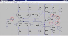
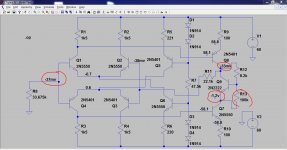
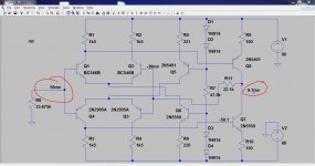
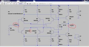
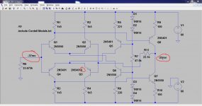
Well simulating with different devices just gives a low offset as expected. Change any input device and the offset alters.
Here the C version is the same transistor but a different model (done by Bob Cordell).
I think the best you can aim for is to match the PNP and NPN pairs as best as possible and then try swapping each pair over one at a time.
If you felt confident you could swap the devices from the other channel to this one and see if the offset is lower.
Attachments
Assuming the circuit works correctly the remaining output DC offset
is mostly influenced by the input stage caracteristics.
What matters is that the differential transistors are VBE matched by pairs,
it s less important that the NPN pair is matched with the PNP pair.
Yes, I would agree with that.
And I think that is is why just checking hfe on a DVM isn't the whole story. It gets it close but not close enough. Given enough devices you should be able to "mix and match" and get it fairly low without having to modify anything (which I wouldn't recommend really).
Yes, I would agree with that.
And I think that is is why just checking hfe on a DVM isn't the whole story. It gets it close but not close enough. Given enough devices you should be able to "mix and match" and get it fairly low without having to modify anything (which I wouldn't recommend really).
Of course the components quality matters given the high voltage
and that leakages can be substancial but even then this design
is flawed from the start and you are left chasing ghosts...
The inputs biaising resistors are of different values and this will
unbalance the input stages voltages since at a biaising current
of 10uA the mismatch in dc inputs voltage will be as much as
100mV for 10K difference in the said resistors leading to
output DC voltages of the same order...
So the bias not only become Vbe dependant but also largely
Hfe dependant , hence you are left with finding input transistors
that are accurately...mismatched !!!...
All in all , quite a nightmare...
The inputs biaising resistors are of different values and this will
unbalance the input stages voltages since at a biaising current
of 10uA the mismatch in dc inputs voltage will be as much as
100mV for 10K difference in the said resistors leading to
output DC voltages of the same order...
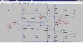
That would be a logical assumption but it doesn't seem to work like that for this type of configuration. Different input bias current don't seem to alter the offset. I tried 10k and 100k (now thats unbalanced) yet the offset is still in single mv figures. It does seem to purely rely on the matching of the semiconductors.
Attachments
- Status
- This old topic is closed. If you want to reopen this topic, contact a moderator using the "Report Post" button.
- Home
- Amplifiers
- Solid State
- Help Needed: Excessive DC Offset/Imbalance - Rotel RB-990BX Power Amp