Hi guys,
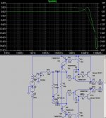
here is a small amplifier I have been fiddling with for a while.
It is up and running on a breadboard right now. The idea is to use high-voltage integrated op-amps such as the OPA551, OPA552, LME49860 etc. to simplify the circuit (no discrete input-diff./VAS stage). These IC's feature supply voltages as high as 40V to 60V.
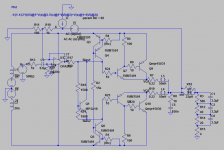
The amplifier shown fits on a 11x5cm (27,9x12,7 inch) PCB using 1206 SMD parts for most resistors and capacitors. I plan on making a small 5.1 surround amplifier for my PC using 6 of these boards on a common heatsink. Output power will be around 20W.
It was extremely difficult to stabilize the CFP output stage. All the usual tricks were tried:
-resistor between driver-E and output-C to lower feedback (this helped, but only using high-value resistors that introduced crossover distortion)
-high value base stopper resistors (this also helped, but limits output voltage swing)
-capacitors between B and C of both the driver and output transistors (never had any success with these)
Now the interesting part: Replacing the 0.22R wirewound emitter resistors with some ceramic-box type resistors immediately made the amplifier stable without *any* of the remedies above. This was also confirmed by simulating loop gain using Middlebrook: With the 50nH series inductance shown, phase margin is about 70°. With around 1mH the amp is oscillating. I have yet to buy a decent inductance meter to confirm the first type of resistors really had such high inductance but from what I have read it seems plausible.
How would I go about simulating loop gain of the *CFP stage alone*? Can I use Middlebrook methode also?
here is a small amplifier I have been fiddling with for a while.
It is up and running on a breadboard right now. The idea is to use high-voltage integrated op-amps such as the OPA551, OPA552, LME49860 etc. to simplify the circuit (no discrete input-diff./VAS stage). These IC's feature supply voltages as high as 40V to 60V.
The amplifier shown fits on a 11x5cm (27,9x12,7 inch) PCB using 1206 SMD parts for most resistors and capacitors. I plan on making a small 5.1 surround amplifier for my PC using 6 of these boards on a common heatsink. Output power will be around 20W.
It was extremely difficult to stabilize the CFP output stage. All the usual tricks were tried:
-resistor between driver-E and output-C to lower feedback (this helped, but only using high-value resistors that introduced crossover distortion)
-high value base stopper resistors (this also helped, but limits output voltage swing)
-capacitors between B and C of both the driver and output transistors (never had any success with these)
Now the interesting part: Replacing the 0.22R wirewound emitter resistors with some ceramic-box type resistors immediately made the amplifier stable without *any* of the remedies above. This was also confirmed by simulating loop gain using Middlebrook: With the 50nH series inductance shown, phase margin is about 70°. With around 1mH the amp is oscillating. I have yet to buy a decent inductance meter to confirm the first type of resistors really had such high inductance but from what I have read it seems plausible.
How would I go about simulating loop gain of the *CFP stage alone*? Can I use Middlebrook methode also?
Attachments
This looks very similar to something I am building. I used even the same transistors MJE15028/29. I have noticed the following:
1) I cannot use high currents on a breadboard - any component's pin that carries over 100mA needs two parallel connections to split the current, else the contact resistances cause voltage drops which would not exist on a soldered circuit. For example I had to solder two separate pins on the in and out pins of an LM317 (4 pins total plus 1 for the reference pin) in order to see how the circuit would behave with currents of 300-400mA.
2) I noticed that my CFP output stage would oscillate badly when using 0.22 Ohm resitors, but the oscillation would go away with 0.27 Ohm resistors. The 0.27 Ohm resistors had a larger body.
3) I solved myriads of HF contamination and oscillations by adding a 100pF cap between B and C of the driver transistors ( but not the output transistors ). On a PCB design I had to increase the caps to 600pF. However on the breadboard, adding too much capacitance would make things worse. Oscillations also depended on the load being driven.
4) When driving a high resistive load (8 Ohm, +/- 8 Volts) I had to increase the bias to about 100mA to clean up the output curve. Else the crossover distortion produces many HF harmonics which can be seen easily on the scope.
5) When driving a heavy inductive load (a transformer instead of an 8 Ohm resistor) I needed the addition of a zobel of 1R / 18nF at the output to stop HF harmonics appearing.
6) I have no 10R series resistors as in your schematic - are these shown provisionally after your comments about reduced output swing?
7) I have paralleled output transistors with 0.15R resistors at their emitters for balancing. You do not appear to have any emitter resistors.
I do not know how to simulate these HF oscillations - the simulation looks perfect but the breadboard or PCB is another story completely.
@Gajanan
u're wrong the mentioned ICs are for audio use and have exceptionally low THD. You can easily buy them on Ebay if your distributor doesn't source them.
I don't like chipamps because a.) very little can be learned by turning the datasheet schematic into a PCB and b.) unlike op-amps, these are special integrated circuits which might be hard to replace if they run out of production.
@akis
Can you plz post a schematic?
Concerning the oscillations, my assumption about the emitter resistors was plain wrong. They have nothing to do with the problem and the amplifier is now running fine with the wirewound resistors. Replacing these with expensive Isabellenhütte low-inductance (<40nH) resistors also didn't cure the problem.
I disassembled one of the wirewound resistors - they contain only 4 windings and inductance is probably below 1uH. The amplifier will be become unstable with inductance of around 1mH, so unless much higher value resistors are used, these are very unlikely to cause problems. The oscillation problem was due to an error in the bias circuit which is now fixed.
The amplifier is built on an breadboard and was tried with peak currents of 1.2A without problems.
"I have no 10R series resistors as in your schematic - are these shown provisionally after your comments about reduced output swing?"
No, these are very important base stopper resistors that you should definetly use! I was refering to resistors between driver emitter and output transistor collector. These lower feedback of the CFP stage, but they also increase crossover distortion and reduce voltage swing. I have removed these resistors after fixing the bias circuit problem.
It is very important to make the op-amp slower than the output stage, otherwise oscillations are bound to occur.
Instead of base stoppers I have used B to C caps. I will try the base stoppers tomorrow to see if these can possibly replace the caps. My schematic is nothing special, simply a current amplifier with compund pair to achieve low distortion and low voltage loss. I have used paralleled MJE15028/29 or single, but oscillations remain the same and only the caps can remove them.
My op-amp is a 200KHz oscillator - I am not sure I understand what you mean by the op-amp needing to be slower than the output stage, are you talking about slew rate?
My op-amp is a 200KHz oscillator - I am not sure I understand what you mean by the op-amp needing to be slower than the output stage, are you talking about slew rate?
@macplauder: So you've got the stability problem resolved? If so, what was the fix? Increase R17 from pF to tens of pF to satisfy the control bandwidth < output stage bandwidth stability constraint? The OPA55x are slow enough I wouldn't expect them to need much bandwidth reduction but would expect an LME49860 would. The schematic in post 1 doesn't show any bypass caps on the supplies but I assume there's good bypassing on the op amp so that it's not going unstable due to supply inductance and that the Siziklais are also well bypassed. (Back when I taught BJT device classes my students would try to run their designs off a lab supply without any bypassing on the breadboard and have all sorts of stability problems. ") )
)
I've had plans for a similar amp for some time---8-SOIC single op amp, 0805s, Darlingtons, and about 10W---but have been busy with other projects and haven't built it. The rule of thumb I'd arrived at was op amp's inner feedback loop needs to deliver GBP = (0.5 to 1.0) fT of the output transistors. Given process variation in GBP and fT I'm unclear on how much less below fT one needs to set the inner loop for to ensure stability---haven't got round to setting up the sims and doing parameter sweeps.
As a data point I've built a different design with GBP = 0.6 fT on datasheet specs and it was stable from the first solder up (8-SOIC single op amp, 1206 build, 10 ohm + 100nF zobel). But one amp channel isn't exactly a statistically significant result.
)I've had plans for a similar amp for some time---8-SOIC single op amp, 0805s, Darlingtons, and about 10W---but have been busy with other projects and haven't built it. The rule of thumb I'd arrived at was op amp's inner feedback loop needs to deliver GBP = (0.5 to 1.0) fT of the output transistors. Given process variation in GBP and fT I'm unclear on how much less below fT one needs to set the inner loop for to ensure stability---haven't got round to setting up the sims and doing parameter sweeps.
As a data point I've built a different design with GBP = 0.6 fT on datasheet specs and it was stable from the first solder up (8-SOIC single op amp, 1206 build, 10 ohm + 100nF zobel). But one amp channel isn't exactly a statistically significant result.
The rule of thumb I'd arrived at was op amp's inner feedback loop needs to deliver GBP = (0.5 to 1.0) fT of the output transistors.
Thanks!
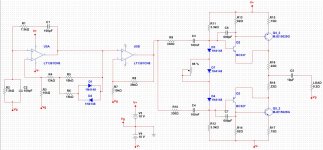
This morning I experimented with 10R base stoppers in my PCB test platform (ie no breadboard weirdness), and they did absolutely nothing to stem the oscillations of the compound pair under load and driven close to the rails from the op-amp and without any global feedback. However placing a 1/10 resistor in series at the output of the op-amp (R9/R10) helped reduce the oscillations visibly, albeit with a small voltage loss at the load. In the end it is only the caps C6/C7 that stop the oscillations completely. There are no oscillations under no load and the test load is purely resistive. To drive an inductive load I have used a 1R/18nF Zobel at the output (not shown on schematic).
I attach a very simplified schematic.
I attach a very simplified schematic.
Attachments
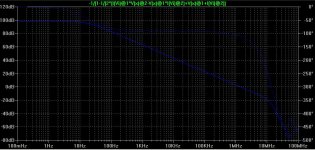
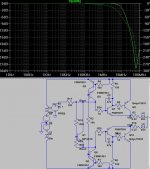
The first pic shows the loop gain plot; phase margin is 70° with 40nH series inductance on the emitter resistors. The second plot shows the same circuit with 10mH inductance. So we can see that inductance is a possible source of instability, but this is very unlikely to happen with reasonably sized wirewound emitter resistors. If in doubt, 1R carbon resistors can be placed in parallel.
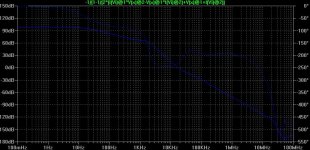
With 2pF compensation for the op-amp, phase margin is improved to 80°.
GBW of the OPA552 is 12MHz and fT of the MJE15028/30 is 30MHz. Driver fT is 150MHz. The output stage has a gain bandwidth of around 28MHz but shows a nasty peaking in gain at 15MHz (3rd pic). Adding 47pF between driver B-C gets rid of this anomaly and limits bandwidth to 12.5MHz (4th pic). So it can't hurt to use these caps and also a small compensation cap (~2pF) to slow down the op-amp a little.
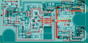
I've also attached a PCB layout for this circuit (4,2x2,1 inch for a single channel) using mostly wired parts and some 1206 SMD resistors and electrolytics. The FMMT491 transistor is only available as SOT23 AFAIK. There's bypassing for the output stage and op-amp, and also each channel gets a simple zener+emitter follower "regulator" for a clean supply voltage. There's a NAiS TQ2SA-5V relais to switch between speaker and HP output. I plan on using this for a 5.1 amplifier for my PC; it would also allow for 5.1 headphones.
@twest820
Your GBP formula is a nice rule of thumb. The 150x/FMMTx91 transistors were chosen to make sure the output stage has higher bandwith so that the op-amp is always in control. I like to visualize this by imagining that a slower output-stage would cause the op-amp to servo a feedback signal which has so much phase shift that it is always "too late" (well a phase shift isn't a delay really, but anyways).
The source of my oscillations was simply a wiring error on the breadboard. It simply wasn't the circuit shown in post #1. I didn't observe any oscillations since correcting the wiring.
With 2pF compensation for the op-amp, phase margin is improved to 80°.
GBW of the OPA552 is 12MHz and fT of the MJE15028/30 is 30MHz. Driver fT is 150MHz. The output stage has a gain bandwidth of around 28MHz but shows a nasty peaking in gain at 15MHz (3rd pic). Adding 47pF between driver B-C gets rid of this anomaly and limits bandwidth to 12.5MHz (4th pic). So it can't hurt to use these caps and also a small compensation cap (~2pF) to slow down the op-amp a little.
I've also attached a PCB layout for this circuit (4,2x2,1 inch for a single channel) using mostly wired parts and some 1206 SMD resistors and electrolytics. The FMMT491 transistor is only available as SOT23 AFAIK. There's bypassing for the output stage and op-amp, and also each channel gets a simple zener+emitter follower "regulator" for a clean supply voltage. There's a NAiS TQ2SA-5V relais to switch between speaker and HP output. I plan on using this for a 5.1 amplifier for my PC; it would also allow for 5.1 headphones.
@twest820
Your GBP formula is a nice rule of thumb. The 150x/FMMTx91 transistors were chosen to make sure the output stage has higher bandwith so that the op-amp is always in control. I like to visualize this by imagining that a slower output-stage would cause the op-amp to servo a feedback signal which has so much phase shift that it is always "too late" (well a phase shift isn't a delay really, but anyways).
The source of my oscillations was simply a wiring error on the breadboard. It simply wasn't the circuit shown in post #1. I didn't observe any oscillations since correcting the wiring.
Attachments
This morning I experimented with 10R base stoppers in my PCB test platform (ie no breadboard weirdness), and they did absolutely nothing to stem the oscillations of the compound pair under load and driven close to the rails from the op-amp and without any global feedback. However placing a 1/10 resistor in series at the output of the op-amp (R9/R10) helped reduce the oscillations visibly, albeit with a small voltage loss at the load. In the end it is only the caps C6/C7 that stop the oscillations completely. There are no oscillations under no load and the test load is purely resistive. To drive an inductive load I have used a 1R/18nF Zobel at the output (not shown on schematic).
I attach a very simplified schematic.
Weird way of doing things and I can image distortion being high?
I can't want I haven't built one with the OPA445 yet only with a single NE5534 on 20V rails. I have mimicked STD03N/Ps with discrete components, one HFE category is 8000 and over so don't need anything in between them and the Op amp and I have proved this on the bench. I added a second OPA445 for added loop gain to get that distortion down but it isn't really needed as they are expensive. Bias is 96mA.


Weird way of doing things and I can image distortion being high?
Why weird?
I do not have the rig to measure distortion, I just look at the curve on the scope and am happy when it looks clean and when the output shape on load matches the input shape. I cannot simulate it either - none of the oscillations were evident on the simulator. many designs look perfect in simulation when in fact they suffer from temperature instability, oscillations, variation of components values etc.
@akis
I also don't understand your circuit. What is the purpose of the first op-amp?
What is C3/C4 needed for? The bias spreader already puts the required VBE between the transistor bases, so there is no need to AC couple a signal to both of them. Also the feedback loop is not around the output stage which increases distortion (unless the output stage is very linear at first).
Ah, that makes more sense. Easy fix too.The source of my oscillations was simply a wiring error on the breadboard.
Interesting sims; thanks for sharing.Yes, so far as I know SOT23 is the only package for FMMTx91. I looked at several of the Diodes BJTs for my amp but ended up designing for the Sanken STD03N and STD03P for bias stability and small size (the layout I have sitting around fits two channels into a 2x3 inch two layer PCB including 15,000+uF per rail; not bad). Unfortunately Sanken doesn't publish models for them and characterizing the 03Ps I picked up for cheap hasn't happened--no fT spec but Sanken's other Darlingtons are in the 45 to 80MHz range so hopefully the STD03s are fairly fast.
2pF is probably comparable to the stray capacitiance on the board. Disengages the outer loop at what, 100MHz? The AD797, LME49713, LME49990 are the only audio op amps I know of where that might matter. Something I've been contemplating though is lowpassing in feedback loops. That's as simple as stacking a cap on top the feedback resistor and a first order roll off at, say, 100kHz provides a significant reduction in the bandwidth the op amp will try to control the output stage over. Good for noise rejection and avoiding slew rate consumption by high frequency wibbles so that the excess loop gain stays fully engaged over the audio bandwidth. However, the LME49710 channel I'm operating without any feedback filtering is already better than any of the measurement gear I have access to. So if filtering were to help it out I've no objective way to verify that.
Thanks.Your GBP formula is a nice rule of thumb.
@akis
I also don't understand your circuit. What is the purpose of the first op-amp?
What is C3/C4 needed for? The bias spreader already puts the required VBE between the transistor bases, so there is no need to AC couple a signal to both of them. Also the feedback loop is not around the output stage which increases distortion (unless the output stage is very linear at first).
My circuit is similar to yours in that there is a push pull with compound pairs and unwanted oscillations. That is where the similarity ends I think.
Why weird?
I do not have the rig to measure distortion, I just look at the curve on the scope and am happy when it looks clean and when the output shape on load matches the input shape. I cannot simulate it either - none of the oscillations were evident on the simulator. many designs look perfect in simulation when in fact they suffer from temperature instability, oscillations, variation of components values etc.
You can't see millivolts on top of volts on a scope so you can't see the distortion, it's very hard. There's no point in C3, C4 and R10 there should be global closed feedback to minimize distortion perhaps use one BD139 instead of three diodes? It makes for easier mounting and overall simplifies the circuit. You can at least simulate distortion in multisim as well as use frequency gens so you don't need to make them. Yes simulation is way off real life but it can give use proof of concept.
- Status
- This old topic is closed. If you want to reopen this topic, contact a moderator using the "Report Post" button.
- Home
- Amplifiers
- Solid State
- High-voltage-opamp based amplifier