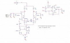
I am able to calculate the gain of the differential pair with the darlington pair along with the input and output resistances. however I'm having trouble understanding how the op amp works once its connected to the differential amplifier collector terminal.
From what i understand, the output resistance of the Differential pair is 3.75K (the collector resistance) and that resistance would appear at the operational amplifier.. meaning the gain will be dependent on the ratio of the op amp resistance of 5k ( R15) and the input resistance 3.75K.
However that it incorrect. what idea am i missing ? [ i know if i assume that the collector resistance is 5k . I arrive at the correct solution according to the simulation (Av=5) ]
(Please note the the written equation is not meant for this schematic.)
From what i understand, the output resistance of the Differential pair is 3.75K (the collector resistance) and that resistance would appear at the operational amplifier.. meaning the gain will be dependent on the ratio of the op amp resistance of 5k ( R15) and the input resistance 3.75K.
However that it incorrect. what idea am i missing ?
[ i know if i assume that the collector resistance is 5k . I arrive at the correct solution according to the simulation (Av=5) ](Please note the the written equation is not meant for this schematic.)
Attachments
Last edited:
1. Your current mirror needs some help.
Disconnect the base of Q7 from Q6
Connect the base of Q7 to the collector of Q7.
Remove Q6 and connect the emitter of Q5 to R3.
2. V2 negative source...is the polarity correct?
Is it a "generic supply" that you set to -15V or is it a 15V supply and you should reverse the symbol to get -15V?
In the interest of having a clear schematic, I would set it at +15V and reverse the symbol, but that is just me.
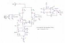
Note 1. A current source with a shunt resistor is the same as a voltage source with a series resistance. ( at a specific value )
Note 2. The transistor stage is a voltage to differential current converter.
Note 3. The op-amp stage is a differential voltage to voltage converter.
Let's make a few assumptions for easier calculations.
Transistor gain is high enough that B is 1 ( not .999xxx or something)
The current mirror is infinite impedance.
C5 (I don't think it is needed) and R34 are not in the equation.
calculations ignore DC values
R10 and R11 are not in the calculations
Vbe does not change as a result of signal
Here we go:
If the input is raised by 0.1V the collector of Q5 is raised by 0.05V
Q1/Q2 current increases by 50uA ( 0.05V / 1000R )
Q3/Q4 current decreases by 50uA ( 0.05V / 1000R )
( Note 2.)
50uA with a 3750R shunt can be represented by a 0.1875V source ( 50uA * 3750R ) with a 3750R series impedance. ( Note 1. )
This gives us ( differentially ) a 0.375V signal with an equivalent of 3750R in each leg.
Now it is easier to calculate the op-amp gain stage.
In the Q1/Q2/U3A+ip path the signal would get 5000 / ( 3750 + 5000 ) or 0.571429 of any signal. ( Straight voltage divider. )
In the Q3/Q4/U3A-ip path the signal gain is calculated as an inverting amplifier as 5000 / 3750 or 1.3333...
So overall differential gain of that stage would be 0.571429 * 1.3333... = 0.761905
( Note 3. )
The first stage gave you 0.375V for 0.1V input or a gain of 3.75
Multiplying the two gains together would give you 2.857
IMHO
What number did the simulation get?
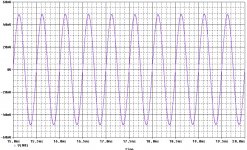
So the simulation gave you a gain of 3.39
I will have to re-think my analysis of the circuit.
There is another way to approach this.
The two first stage outputs do not see the same load and will get different outputs.
I will have to think some more but have to go now.
later
I will have to re-think my analysis of the circuit.
There is another way to approach this.
The two first stage outputs do not see the same load and will get different outputs.
I will have to think some more but have to go now.
later
- Status
- This old topic is closed. If you want to reopen this topic, contact a moderator using the "Report Post" button.
- Home
- Amplifiers
- Solid State
- Help Needed with simple hybrid microphone pre-amplifier