Have you ever measured the actual signals sent to your speakers?
I have measured my signals, often.
I have stated quite a few times that my average listening levels are well below 1W.
Typically I see average levels of around 0.5Vac to 2Vac.
I can convert that to SPL if I want, but in the context of this discussion I don't need SPL.
I am trying to point out that the peak to average ratio of most music types (~12dB to >30dB are frequently posted/published) is way above the 30W to 5W ratio (<8dB) you have mentioned.
If you re-play music at average levels of ~5W with a 30W amplifier then I can virtually guarantee that your are listening to clipped signals. Low distortion of the signal whether due to good amplifier design or good source material does not enter the discussion if you habitually clip your signal before you send it to your speaker/s.
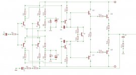
maybe fixed
Hi All..
Thankyou for your help so far ..
Well i managed to find some time to hopefully fix the brokem scem i posted .. would someone please look over it to see if i have made a pigs ear of it . i will re post the original so you wont have to keep going back to the first post..
Kind Regards Mark PS please ignore the changed location numbers
Attachments
Have you ever measured the actual signals sent to your speakers?
Sure
")
Now I understand what you are talking about. I believe that you also understand what I was talking about
The front end is not accurately calculated and as such it wont
perform correctly.
Particularly , there will be big VAS current variation with temperature
wich will render the output stage quiescent current variable as well but
with even larger amplitude that may well turn in thermal runaway.
perform correctly.
Particularly , there will be big VAS current variation with temperature
wich will render the output stage quiescent current variable as well but
with even larger amplitude that may well turn in thermal runaway.
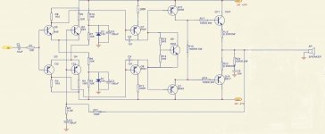
I get nears as dam it 67.6 that seems very high . the amplifier does seem to have quite a high gain but im not sure it is that high. Also you mention thermal runaway The 5551 used as bias transistor is between output devices on the main heatsink will that help!! if i worked it out corectley the cutoff frequency is very close to 1Hz.. if we devide the 67.6 by 2 we get near enuff to 33 that sounds more like it to me . however still a little higher than i would like
Last edited:
In principle it will only increase the current of the said transistors
but the 2N5401/5551 do not have enough thermal dissipation
capability at such a place when it comes to drive a double
emitter follower output stage.
You can use BD139/140 or better 2SA1360/2SC3423 wich are more linear.
Also , for biaising the output stage replace R20 (1K8 in post 46)
by a 1K resistor in serial with a 1K trimmer that will be set at
max resistance value before doing the first power on.
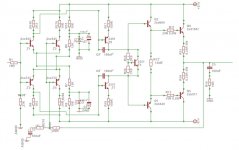
re post 50 & sch in post46.
What signal do you have to drive the power amplifier?
What is your target maximum signal out of the power amplifier?
Divide output by input and you arrive at your required gain.
That gain is defined by ~R300/R210
eg.
Maximum input signal from CDP = 2.2Vac.
Maximum input signal from FM radio = 700mVac.
Maximum speaker signal = 28Vac. (equivalent to 100W into 8ohms).
The CDP will require some attenuation to avoid repeated clipping of the signal , expect at least -10dB.
Required gain is 28/0.7 = 40.
Therefore R300/R210 ~ 40times. i.e. if R210 = 1k5, then R300 should be ~ 60k. Use 56k or 62k
That then fixes R430 @ the same value.
The input filter can now be set using the R430 value you have adopted.
Last edited:
Thankyou Andrew.
here are the specs of the dac i use it is my only source...
Line Outputs
max output level +2dBV (monitor off), +8dBV (monitor on
signal to noise ratio -105dB, A-weighted, max. gain
dynamic range 105dB, A-weighted, max. gain
THD + N 0.002% (-94 dB), 1kHz, -1dBFS, max. g
frequency response 20Hz to 20kHz, -0.2 / +0.1dB, max. gain
output impedance 100 ohms
crosstalk < -110dB, 1kHz, channel-to-channel
Regards Mark
I have managed to read a little of Selfs power amplifier design book.. Could i use a current mirror on the input section. i have so far only found examples with the single LTP. If it is possible i can fit a current mirror in the place of the two resistors as they are in a nice place on the board to do so.. I really like the sound of this amplifier . And will be using it as a learning exercise .. also the emmiter resistors on the output 0.25 ohm.. can they be reduced to .1ohm ???
Hi Nico.
Forget i mentioned the changing the 0.25 for 0.1. I had another little read of Selfs book and it mentions a lower resistance lowers the distortion But that is regarding CFP outputstage and not EF2. Also i noticed another problem maybe? the bias transistor is close to the heatsink but not quite touching it.. after reading Self i understand the thermal issues with an EF2 stage need etra care. i propose to stick the bias transistor to one of the output devices to hopefully improve this area..
Kind Regards Mark
A lot of people (on DIY) stick this transistor on top of one of the output devices. I have seen this a lot in the threads here.
I don't subscribe to this and believe it is best to tie this transistor onto the heat sink so it responds slowly to the temperature variation a form of hysteresis.
Tying onto one of the output transistors can introduce thermally generated distortion in that the thermal compensation reacts quickly to one transistor but slowly to the other thereby distorting or compressing the output signal.
This is measurable, but maybe not audible at lower temperatures.
buy some sot23 transistors.
Glue one sot23 with the legs sticking out/up, to the collector leg of an output BJT.
Use the legs of the sot23 for your Vbe multiplier.
This gives a much quicker response to Tj changes and helps maintain the optimum bias level. Not as good as the NJLs from ONsemi, but far better than using the heatsink coupled multiplier.
Nico,
you'll gather from my reply, that I disagree with your philosophy.
I Nico .
I did think about hysteresis. I also read that the Upper surface of output devices is the hottest part opposed to the heatsink. I also read that EF2 is more critical of the bias point .. Now to do some more reading as here is a compromise . Wich is going to give less distortion..
1: The way it is now with very loose thermal coupling ( poor bias tracking ?)
2: Affix bias transistor to one output device ( only sensing heat of one output device )
3: Use NLJ,s insted of existing output devices ( very good thermal tracking of bias )
4: Maybe it is possible to use a bias transistor on both output devices and get an average of both just like on a heatsink with the bias transistor fitted between the devices directly to the heatsink.
Kind Regards Mark
Hi Andrew..
Looks like i have opened a can of worms. . im begining to come to the conclusion that most every component change in an amplifier raises lots of other conciderations and has an affect on other parts of the circuit .. The amplifier in question was gained very cheaply and sounds very pleasing. as this is a working amplifier it helps me relate the theory to the practical element i find this the best way for me to learn .. I think i need to make a list and prioritise the modifications i would like to make .
The effect on lowering distortion by using current mirrors " low cost transistors "
seems like one of good value . however this will alter the gain of the front end.
and therfore the overall gain of the complete amplifier.. Is it possible to alter the gain of the front end only, to bring it to a level the next stage can deal with .. Maybe i have this all wrong . please bear with me as the learning curve is starting to get steeper the more i start to learn..
Kind Regards Mark
- Status
- This old topic is closed. If you want to reopen this topic, contact a moderator using the "Report Post" button.
- Home
- Amplifiers
- Solid State
- Front end help