So I actually started this project a few months ago but to personal circumstances I decided to not continue with the project. Since them I have had quite a few PMs regarding the PCBs so just lately I have designed a new board which I have got made and will be testing tomorrow evening. After I received the boards I noticed a few niggles which needed ironing out and after playing around tomorrow to finalize values and layout I will get the latest revision made and if all good then I will get 100 made and sell however many people want on here then keep whatever's left.
Here is the latest PCB and schematic (with two pairs of ALF16N16W/P type). Estimated power should be around the 400Wrms mark into 8R and 4R depending on how you set your PSU up.
Intended heatsink http://uk.farnell.com/ohmite/ra-t2x-25e/heatsink-to-220-218-247-black/dp/2097683?Ntt=RA-T2X-25E.
LINK to original thread.
Latest revision PCBs...


I'll get some pics of the current boards tomorrow.
Thanks
Boscoe
Here is the latest PCB and schematic (with two pairs of ALF16N16W/P type). Estimated power should be around the 400Wrms mark into 8R and 4R depending on how you set your PSU up.
Intended heatsink http://uk.farnell.com/ohmite/ra-t2x-25e/heatsink-to-220-218-247-black/dp/2097683?Ntt=RA-T2X-25E.
LINK to original thread.
Latest revision PCBs...
I'll get some pics of the current boards tomorrow.
Thanks
Boscoe
Last edited:

Wow, this is a very interesting project, and a very compact layout. I've been looking for a simple and compact amp board that has good THD above 1kHz, and this has the potential to fit that requirement nicely.
Looking forward to hearing the results of the proto board testing...
In any case, I would be interested in a dozen (12) of the final boards.
Also, is any one else interested in purchasing populated boards from an assembly company? I am not looking forward to smd soldering...
-Charlie
Looking forward to hearing the results of the proto board testing...
In any case, I would be interested in a dozen (12) of the final boards.
Also, is any one else interested in purchasing populated boards from an assembly company? I am not looking forward to smd soldering...
-Charlie
Last edited:
Sorry this is late but I did go out for a few beers after work yesterday!
Unfortunately all my work on this project has to be done at the office after 5:00PM so I only get less than an hour to work at a time. After making all the test cables and getting the amp on the sink I had hardly any time to do and tests but the prototype does work! I did get sound from it into a speaker!
Also the test PSU I was using stopped working so now I only have a switching lab supply which is no good whatsoever so measurements so I'm going to make a large 800VA bench PSU at +/-60V which I hope to get done this evening along with any other niggles (hopefully none) so I can update the layout and get it sent off to be fabricated. I can then test it and once all is good I can get the full quantity made and sold to you guys.
So my estimated time of getting the final boards to sell is two weeks being optimistic so done be upset if it take three weeks!
Schematic...
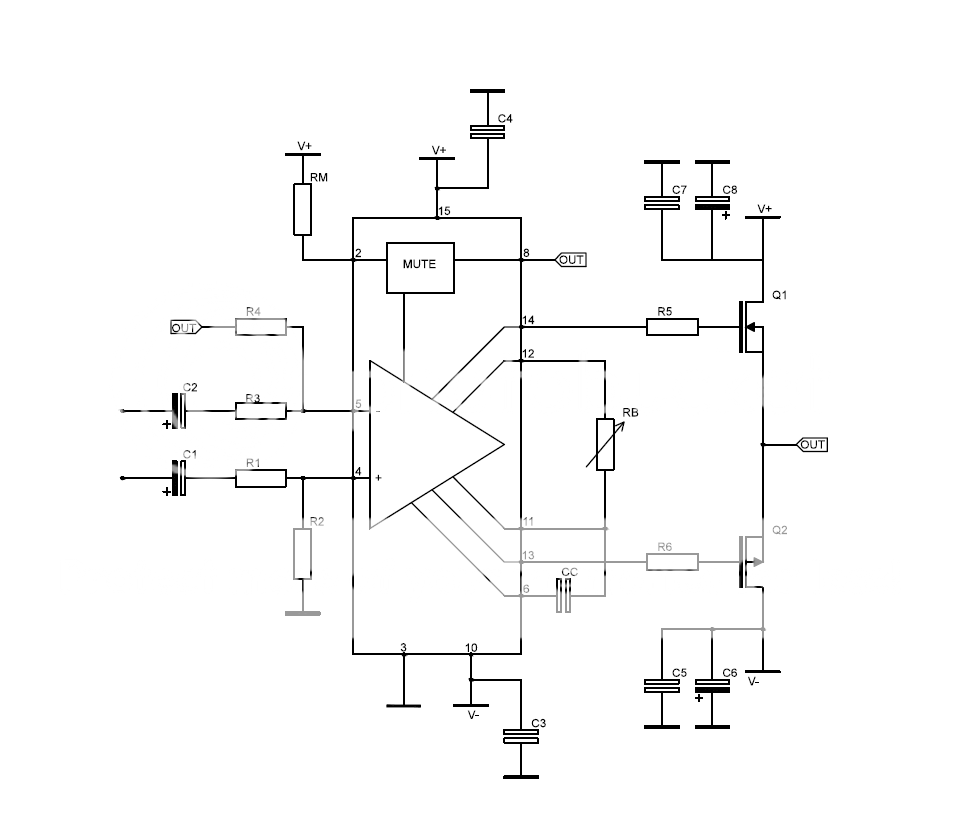
Now there are no small coupling caps on the output devices, two pairs of output devices and a zobel filter on output made up of 10R and a 100nF cap to be added to the layout. C1 and C2 are also non polar with C2 being grounded for single ended, would people want the option of a balanced input?
This schematic may change depending on tonight's testing.
Thanks
Boscoe
Unfortunately all my work on this project has to be done at the office after 5:00PM so I only get less than an hour to work at a time. After making all the test cables and getting the amp on the sink I had hardly any time to do and tests but the prototype does work! I did get sound from it into a speaker!
Also the test PSU I was using stopped working so now I only have a switching lab supply which is no good whatsoever so measurements so I'm going to make a large 800VA bench PSU at +/-60V which I hope to get done this evening along with any other niggles (hopefully none) so I can update the layout and get it sent off to be fabricated. I can then test it and once all is good I can get the full quantity made and sold to you guys.
So my estimated time of getting the final boards to sell is two weeks being optimistic so done be upset if it take three weeks!
Schematic...
Now there are no small coupling caps on the output devices, two pairs of output devices and a zobel filter on output made up of 10R and a 100nF cap to be added to the layout. C1 and C2 are also non polar with C2 being grounded for single ended, would people want the option of a balanced input?
This schematic may change depending on tonight's testing.
Thanks
Boscoe
Is the Signal Ground/Return separate from the Power Ground?
Are Pins 10 & 15 connected via a series pair of HF (ceramic) decoupling capacitors?
The heatsink data shows ~30C rise for a 3.7W dissipation (150Vdc @ 24/26mAmax)
That puts the 1" sink at about 60°C. I would recommend a bigger sink.
I have OPC's version and the sink in that runs a bit hot right next to some electrolytics. And I'm only using 95Vdc
Last edited:
The Bias+ and Bias- should be connected to a bypass capacitor (across the potentiometer). (Should be a.c. coupled)
Yes sorry thsi is an old schematic, it's bypassed with 22pF.
Is the Signal Ground/Return separate from the Power Ground?
Are Pins 10 & 15 connected via a series pair of HF (ceramic) decoupling capacitors?
The heatsink data shows ~30C rise for a 3.7W dissipation (150Vdc @ 24/26mAmax)
That puts the 1" sink at about 60°C. I would recommend a bigger sink.
I have OPC's version and the sink in that runs a bit hot right next to some electrolytics. And I'm only using 95Vdc
Yes 100nF ceramic 100V decoupling.
The sink I'm using has a thermal resistance of 4.8C/W, with a dissapation of 3.7W and ambient temp of 30C that's only 47.76C. Better than The Wire's heatsink at 11C/W. This sink also has better mounting options.
Again thanks everyone for the questions keep them coming it makes ironing out niggles far easier.
Is the Signal Ground/Return separate from the Power Ground?
Are Pins 10 & 15 connected via a series pair of HF (ceramic) decoupling capacitors?
The heatsink data shows ~30C rise for a 3.7W dissipation (150Vdc @ 24/26mAmax)
That puts the 1" sink at about 60°C. I would recommend a bigger sink.
I have OPC's version and the sink in that runs a bit hot right next to some electrolytics. And I'm only using 95Vdc
I'm no amplifier designer, but I have a couple of comments (I would like to learn about this stuff, so if I am way off please let me know):
- Regarding heat from the LME49830 - can you mount it so that it can be on the same heatsink as the output devices? This would require a complete redesign of the layout, but this would be the best way to dissipate heat from it (so it seems to me) and not one of those small independent heat sinks that you are using now.
- It would be nice to provide a jumper so that people could access the MUTE pin if they so desire. This this wouldn't take up much space and would let the user MUTE the amp at start up. Installing the jumper would connect the current sourcing resistor so that MUTE is always "off".
- 4R7 resistor between Vcc and pin 16. In Cordell's design, the 4R7 is located between the output devices and the Vcc pin supplying the LME49830 driver IC. The bypass caps are on the driver IC side of the 4R7, and there is a direct connection between Vcc and the output devices. This provides some rail filtering for the driver, but not for the output devices, which I think is a better approach. This 4R7 resistor may need to be a macro sized one because of power dissipation, not sure.
- #1 also applies to the Vee connection to pin 10 and the output devices
- you do not show an RF input filter. Perhaps this could/should be done at the inputs (e.g. not on the amp pcb but at the entry to the enclosure)?
- are you are not using pin 8, the Osense? From the LME49830 datasheet:
The Output Sense pin Osense must be connected to the system output as shown in Figure 1. This connection completes the return path to feedback the output voltage to the mute gain circuitry inside LME49830. If the Osense pin is not connected to the output or it is floated, high voltage generated from the output stage may cause damage to the speaker or load.
- you don't use the series output resistors after the output devices, which is recommended when using more than one output device per rail. I believe that these resistors balance the load between the output devices
- I noticed that on your schematic pins 11 and 12 are reversed compared to Cordell's schematic in which Rbias_adjust connects pins 11 and 12 (you show this also) but pin 6 is only connected to pin 12 via a small (20pF) cap. In your schematic, pin 6 connects to pin 11 by a cap (not sure of value), which is the reverse of Cordell but is the same as what is shown the LME49830 datasheet. Not sure here, might not matter, but I noticed the difference.
Sorry if some of my questions are not very intelligent! I just wanted to bring up these issues in case any of them were of concern...
-Charlie
are you are not using pin 8, the Osense? From the LME49830 datasheet:
The Output Sense pin Osense must be connected to the system output as shown in Figure 1. This connection completes the return path to feedback the output voltage to the mute gain circuitry inside LME49830. If the Osense pin is not connected to the output or it is floated, high voltage generated from the output stage may cause damage to the speaker or load.
Ooops, I noticed that you are using the Osense pin! My bad.
OK, one other question from this amp noob - why do I sometimes see amp boards that use this driver IC requiring a higher voltage for the VAS (which I assume is in the driver IC)?
Thanks,
-Charlie
I'm no amplifier designer, but I have a couple of comments (I would like to learn about this stuff, so if I am way off please let me know):
I have Bob Cordell's book "Designing Audio Power Amplifiers". Maybe a little knowledge is dangerous, but he gives a design using the LME49830 driving two pairs of MOSFETs and here I am assuming it is correct. Here is a list of some of the differences I noticed:
- Regarding heat from the LME49830 - can you mount it so that it can be on the same heatsink as the output devices? This would require a complete redesign of the layout, but this would be the best way to dissipate heat from it (so it seems to me) and not one of those small independent heat sinks that you are using now.
- It would be nice to provide a jumper so that people could access the MUTE pin if they so desire. This this wouldn't take up much space and would let the user MUTE the amp at start up. Installing the jumper would connect the current sourcing resistor so that MUTE is always "off".
- 4R7 resistor between Vcc and pin 16. In Cordell's design, the 4R7 is located between the output devices and the Vcc pin supplying the LME49830 driver IC. The bypass caps are on the driver IC side of the 4R7, and there is a direct connection between Vcc and the output devices. This provides some rail filtering for the driver, but not for the output devices, which I think is a better approach. This 4R7 resistor may need to be a macro sized one because of power dissipation, not sure.
- #1 also applies to the Vee connection to pin 10 and the output devices
- you do not show an RF input filter. Perhaps this could/should be done at the inputs (e.g. not on the amp pcb but at the entry to the enclosure)?
- are you are not using pin 8, the Osense? From the LME49830 datasheet:
The Output Sense pin Osense must be connected to the system output as shown in Figure 1. This connection completes the return path to feedback the output voltage to the mute gain circuitry inside LME49830. If the Osense pin is not connected to the output or it is floated, high voltage generated from the output stage may cause damage to the speaker or load.
- you don't use the series output resistors after the output devices, which is recommended when using more than one output device per rail. I believe that these resistors balance the load between the output devices
- I noticed that on your schematic pins 11 and 12 are reversed compared to Cordell's schematic in which Rbias_adjust connects pins 11 and 12 (you show this also) but pin 6 is only connected to pin 12 via a small (20pF) cap. In your schematic, pin 6 connects to pin 11 by a cap (not sure of value), which is the reverse of Cordell but is the same as what is shown the LME49830 datasheet. Not sure here, might not matter, but I noticed the difference.
Sorry if some of my questions are not very intelligent! I just wanted to bring up these issues in case any of them were of concern...
-Charlie
There is no pin 16 and I don't quite understand what your saying about Bob Cordells schematic can you post a link?
A zobel network has been added into the next revision.
I don't need series resistors, these are lateral fets with a negetive temp coefficient and so current share very well.
Again I don't know about Bobs schematic...
you'll need more than 22pF to a.c. couple the bias pins -- something like 22uF
Yes sorry I will check that out tomorrow.
Ooops, I noticed that you are using the Osense pin! My bad.
OK, one other question from this amp noob - why do I sometimes see amp boards that use this driver IC requiring a higher voltage for the VAS (which I assume is in the driver IC)?
Thanks,
-Charlie
The LME isn't able to swing it's output voltage to max rail and so you make the LME rail higher so it's max swing reaches that of the output stage rail. This just decreases a little inefficiency in the output stage but I wanted something simple and so this will be fine.
I will have a look at adding mute.
Overall board size is 90mm x 43mm.
I haven't done any testing today because the PSU took longer than anticipated to make, I should do some measurements on an AP tomorrow morning.
Thanks
Boscoe
Last edited:
- Status
- This old topic is closed. If you want to reopen this topic, contact a moderator using the "Report Post" button.
- Home
- Amplifiers
- Chip Amps
- LME49830 PCBs...