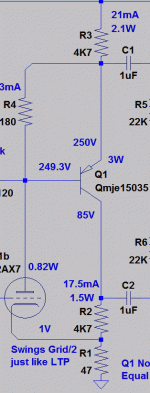
This is what I done with CFB: Attenuate feedback to the cathode.
Making collector gain and impedance equal with Plate+Emitter.
Keep in mind the AX7 plate gives 1/100 feedback, so attenuation
ratio for cathode feedback wants to be set about the same.
"Normal" thing would have been unity gain at the cathode. And
approximate inverted copy at the plate, with unequal impedance.
This was intended a phase splitter for a hybrid amp, if omission
of the irrelevant context of circuit made its function hard to see.
Now we got a concertina splitter with +50/-50 gains. Go figure...
I'm just sayin' this topology has other uses beyond the obvious.
Attachments
Last edited:
If you could see where is my power amp, and the time it ask-me to unplug everything and get-it out, you would understand why i am lazy to do-itthe answer is still on the waiting months later.....
")
In my sim, current feedback, no signal, values are around:
645µa in R1, R2
1.25ma in R6 R29
736µa in R12 R 26
138ma inR21, R22, R24, R23
More thoughts on cfa vs vfb;
Assuming ideal transistors (and no degeneration) and the standard complementary pnp-npn emitter coupled pair for the cfa and a ltp for the vfb (all else being equal) then:
With a increasing input for the vfb the resulting changes in the collector currents still have to sum to 0 (constant tail current), that is equal current changes in the collector currents. Resulting in changes of the 2 emitter voltages of the opposite phase, because of the non-linear vbe-ic then the difference between the 2 emitter voltages from linear will be the source of distortion.
For a cfa with increasing positive input the resulting changes in current do not have to sum to 0. But rather the total bias across the 2 emitters will remain constant. Graphically I think I've convinced myself that this will result in slightly higher positive current change than the negative (pnp) collector current. This positive (npn) current change will also be higher than the vfa as it needs to non-linearly compensate for the smaller reduction in the pnp side transistor (this all assume that both cfa and vfb have current mirrors in both collectors). In the end the cfa net distortion will be less than for a vfb because the difference in the increase positive vbe is smaller than the increase in the the pnp side. That is for a cfa the total non-linear variation will be less.
Strange that a vfb results in "constant current steering" and a cfa in "constant emitter summing voltage".
Thanks
-Antonio
645µa in R1, R2
Hence , there will be about 645mV voltage drop across R1 and R2 ,
not enough to bias the BE junction of Q7/Q9 whose emitter resistors
low value will induce extremely temperature dependant current
once the VAS start to conduct substancialy.
736µa in R12 R 26
This is the VAS quiescent current....
As already said , the VAS work in the edge of class C while the low value
of R12/R26 allow it to supply high current once it enter conduction leading
to high slew rate.
Given the value of R12/R26 , once the VAS is class A biaised its
quiescent current will increase dramaticaly at a rate of 10mA for 100mV
variation of the voltage across the said resistors and will be highly temperature dependant as Q7/Q9 have 2mV/°C VBE variation with temperature, hence the VAS current will vary at a rate of 0.2mA/°C.
The result is that at very small output voltage the amp has
low open loop gain and reduced bandwith.....
Once the VAS conduct , its transconductance rise dramaticaly ,
and the amp bandwith and open loop gain increase accordingly.
If the VAS is biased in class A the amp become instable.
You are right. Just increase those to 1.4K to push the driver quiescent to the same value than original and have a fair comparison ?Hence , there will be about 645mV voltage drop across R1 and R2
Too, i was wrong, telling that the Power Mosfets where IR, they where original Hitachi, i think. Time is so far away, when i constructed this amp and my memory burn-out with time to lower value.
For my previous post (#203), in other words:
For a VFB the equally split collector currents will have follow the input thus the non-linear vbe-ic relationship is seen as distortion from the voltage difference, whereas for cfa the voltage between the emitters will split equally and the collector currents will show the non-linear ic-vbe relationship, these current differences however will add to reproduce the equivelent nearly non-distorted current, since the voltage difference between the output and input is in this case much more linear.
Thanks
-Antonio
As long as we are talking about BJTs, they are driven by a base current.
If you want to drive linearly with voltage, need a base or emitter resistor.
Unbuffered resistive voltage divider can provide this resistance with no
extra parts.
It would be sorta of ridiculous to buffer the divided voltage, then add
back the resistance required for local linearity.
Voltage feedback to me sais "don't use any resistance here", and "rely
upon tons of global feedback to straighten out a local non-linear mess."
But compensating for stability is sometimes complicated by the curve.
With rare exception, I don't see the advantage...
---
Maybe this is a different game when BJTs are not the chosen device?
But even example #201 with a voltage driven triode: Current in the
1st device is held constant by 2nd device of the complimentary pair.
(assuming a resistor across VBE of the second device will be used).
Thus voltage drop across R1 attributed to the 1st device is constant.
There would have been no point to buffer the divider in this instance,
so I didn't bother...
Kenpeter,
I agree with you (except I dont believe this is limited to BJT devices) and as Elvee has already pointed out you can trade open loop gain for local feedback or degeneration.
However my posts were mostly academic, as I stated my conditions to be ideal transistors, no de-generation and all else being equal (i.e. loop gain).
My point was that the ideal cfa-vfb implementations are in some sense at opposite ends of the spectrum. To achieve the same open loop gain as the ltp the cfa would have to have a feedback impedance of Vt/2Ic which would be very low ~5 ohms and not very practical. On the other hand if you increase this feedback resistance to a more practical value of 400 ohms (10Kohm with a gain of ~25) then for the same loop gain the ltp could be degenerated significantly and result in the same distortion.
The trades are there for the desired performance.
Thanks
-Antonio
Easier to weld ?a more practical value of 400 ohms
Easier to weld ?
I don't get it Christophe please explain?
Thanks
-Antonio
You are right. Just increase those to 1.4K to push the driver quiescent to the same value than original and have a fair comparison ?
Too, i was wrong, telling that the Power Mosfets where IR, they where original Hitachi, i think. Time is so far away, when i constructed this amp and my memory burn-out with time to lower value.
A distorsion test would be interesting , just use whatever
soundcard you have , it will be enough up to a few Khz.
As spectral analyzer Visual Analyzer or RMAA should do it perfectly.
Christophe
Thanks wasnt sure.
I was just trying to show what is needed to have the same loop gain between the ltp and complimentary emitted coupled pairs.
This later cfa topology does allow one to theorectically zero out its distortion with emitter resistors to the feedback point.
Thanks
-Antonio
Thanks wasnt sure.
I was just trying to show what is needed to have the same loop gain between the ltp and complimentary emitted coupled pairs.
This later cfa topology does allow one to theorectically zero out its distortion with emitter resistors to the feedback point.
Thanks
-Antonio
I believe in my old LEA. The original amp showed something like 0.008/9 % reduced by something i evaluate as a 10 factor with current feedback (needle was moving too much with the noise to can measure anything).A distorsion test would be interesting , just use whatever
soundcard you have , it will be enough up to a few Khz.
As spectral analyzer Visual Analyzer or RMAA should do it perfectly.
i evaluate as a 10 factor with current feedback
Such estimation cant be right as it involves one order of magnitude
better linearity , yet there is still two stages and the original Crescendo
already almost maxed out the THD numbers that are possible for two
stage topologies.
So either your amp has 20db higher OLG , wich is not the case
or the components did magicaly yield ten times better
built in linearity....
To close the subject, here is a final example showing how misleading preconceptions can be.
This output stage has performances that most aficionados would think as typical of CFB: sub-ppm linearity, output impedance in the microohm range, etc
Yet, it is a pure VFB, but more than that it is an absolute extremist of its kind: the feedback is 100%, and pure voltage mode, and the input by contrast is almost in current mode (sort of). In fact, the exact opposite of CFB.
Think about it...
Attachments
Apart from mundane biasing details, there is one big problem there: it will become a schmitt trigger due to positive reaction.Replace Q8/Q10 by low Z resistances, and common base by common emitter for the input stage, what is-it ?
I don't know, that is one of the many topologies I have investigated, I let you decide.Haw about the bias, is it something close to the Edmond non switching auto bias OPS?
Maybe some day I'll publish a projectCould you give some more information?
- Status
- This old topic is closed. If you want to reopen this topic, contact a moderator using the "Report Post" button.
- Home
- Amplifiers
- Solid State
- Is the CFB topology superior, and why?