Sorry... I did not say that the path i have chosen is my designs is the only way.. there may be numerous way the getting the desired result. what i have seen in my designs is that simple current feedback circuits with good housekeeping is at least for me and my ears a feasible path.
I don't think you can prescribe what is mandatory or not. There are too many Great sounding designs of all types and topologies to make generalizations like that.
In this thread the topic is feedback only, not other parts of the amps, topologies, etc.
Can someone explain why we need extra transistor in FB path if the output impedance from where FB is taken is low Z?
Any nonlinear element inserted in FB path makes the whole regulation process to deal with extra unnecessary corrections that wouldn't be needed if this element wouldn't be inserted. From that point of view CFB is superior to VFB because it deals with less anomalies in a regulation system, in other words regulation formulas are much simpler, considering all the physical laws from subatomic particles up.
Sorry... I did not say that the path i have chosen is my designs is the only way.. there may be numerous way the getting the desired result. what i have seen in my designs is that simple current feedback circuits with good housekeeping is at least for me and my ears a feasible path.
CFB perfectly serves me as well.

The start in CFB designs for me was the thread that lineup started on the Fetizilla. That was a very eye opening design for me... later a found that it was kind of Old news as the Hiraga I so enjoyed when younger also had the CFB approach.
Later The SSA take on the Hiraga evolution took thing a step further, as this type of bridge suspension of the gain takes away some of the single ended circuits limitations. But at the cost of added complexity and further need for extensive housekeeping.
Lazy..one can argue if the non ideal current source of a resistor is better or worse than a extra transistor or Fet. Hence my quest for discussing the pro and cons of the supporting circuit... As in most in life it simply boils down to the execution.
Last edited:
In this thread the topic is feedback only, not other parts of the amps, topologies, etc.
Can someone explain why we need extra transistor in FB path if the output impedance from where FB is taken is low Z?
Any nonlinear element inserted in FB path makes the whole regulation process to deal with extra unnecessary corrections that wouldn't be needed if this element wouldn't be inserted. From that point of view CFB is superior to VFB because it deals with less anomalies in a regulation system, in other words regulation formulas are much simpler, considering all the physical laws from subatomic particles up.
If you are so concern of extra transistor in FB path you can use inverted input in VFB amp as signal input.
can't do.. then you get a real low input impedance or very high impedance and noisy feedback chain
Yes you can, just put a buffer before input. There are simple and excellent buffers as from JLH.
Yet they are not sonically invisible... you just change one set of drawbacks for another.
But inverted shunt feedback circuits can sound good too.. as I said not one true path.
They could have lower distortion then the rest of the amp, so they could be sonically invisible.
That's my point from the beginning of this thread, both in the linear point of view and in the time domain.Can someone explain why we need extra transistor in FB path if the output impedance from where FB is taken is low Z?
Any nonlinear element inserted in FB path makes the whole regulation process to deal with extra unnecessary corrections that wouldn't be needed if this element wouldn't be inserted.
And we both provide exactly the same argues.
But it seems we are talking in a desert, for some contributers.
No one pretend that it is not possible to reach the same level of performance (or better) with other amps, using better parts, other more complex FB implementations (error correction, Nested feedback loops, inverting amps where feedback is applied before - input at low Z etc...).
We need to be serious and compare what can be compared.
What i said from the beginning, providing an example to test-it, is: everything equal around, a current feedback implementation will always give better results than VFB in the same amp topology.
It measure better, and lot of listeners pretend that it sound better.
Last edited:
there are few costs from the "added" diff pair Q - small signal Q at today's hotter bias are running at 100s of MHz ft - meaningless added delay compared to commonly used power output Q with ft from low MHz to low 10s of MHz ft
the better matching of like polarity Q gives better distortion cancelation in a diff pair vs the CFB complementary input
there is no good reason I know of to believe CFB has inherently lower audio distortion for similar number of gain devices, bias levels, compensation - certainly not the 10x factor you claim
I strongly suspect your comparison is "unfair" due to easily "debugged" reasons like bias, compensation, test level differences between the circuits
you refuse to clean up your sim which you claim "proves" your assertion - until then, and we can compare clean sims I see no reason to believe you
I am not dismissing CFA - in fact I use the TPA6120/THS6012 every place it makes sense
Last edited:
I don't know what you are talking about. You are welcome to "clean" anything you want and demonstrate the contrary, or provide any sims of yours to do it.you refuse to clean up your sim
Last edited:
Ok.. then look at it this way.. what is the signal above the differential pair..?? modulated current.. then why not inject the feedback as current modulation, rather than going through a V/I conversion.. that has to pass through not one but two transistors to blend with the signal. You can go through a 1000 sims.. It'll tell you nothing more than common sense can give you just by looking at the nature of things
Devil being in the details, can you show the schematic you are referring to?Ok.. then look at it this way.. what is the signal above the differential pair..?? modulated current.. then why not inject the feedback as current modulation, rather than going through a V/I conversion.. that has to pass through not one but two transistors to blend with the signal. You can go through a 1000 sims.. It'll tell you nothing more than common sense can give you just by looking at the nature of things
But as already stated many times, adding a transistor provides a first order compensation of non-linearities, meaning in practice you get a ~20dB improvement practically for free from the point of view of closed-loop margins, and other parameters
I don't know what you are talking about. You are welcome to "clean" anything you want and demonstrate the contrary, or provide any sims of yours to do it.
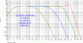
The sims says that the VAS current is negligible and consequently
exponentialy rising with temperature to still a negligible value
of about 180uA at 70°C.
At 0°C the VAS current is so low that the closed loop bandwith
is about 200Hz , rising to 10khz at 20°C , 200Khz at 40°C and
1.5Mhz at 60°C with a slight frequency bump at 1.1mhz
due to the VAS current/transconductance starting to magnify
high frequency poles.
In a few words , this amp will inherently and very audibly
sound much better once it has warmed and the hotter the better ,

though normal VAS current will produce a big peak at a few mhz.
The distorsion figures are nowhere near the 10X claimed
improved ratio , in fact there s no improvement at all
and as a whole it perform not as well as the original
crescendo for most significant parameters.
Attachments
Last edited:
What a misunderstanding of closed loop systems !! (stated many times ?)But as already stated many times, adding a transistor provides a first order compensation of non-linearities, meaning in practice you get a ~20dB
Let look at a differential VFB amp.
The distortion produced by the +V input will be present in the output.
Remove-it from the feedback signal by a similar distortion in opposite phase in the -V stage, and you simply induce this distortion will be removed from the feedback signal, so never corrected by the feedback loop.
Adding this distortion in the signal path, you will correct two times this distortion, so get the same amount, but in phase opposition.
Not at all what i measured on my real amp and with LTSpice. I wonder where is the problem. Models ? Different Spice program ?The sims says that the VAS current is negligible and consequently exponentialy rising with temperature to still a negligible value
of about 180uA at 70°C.
Currents are quite the same in the VFB and the CFB on my LTSPICE.
~300µa in the first stage, ~10ma in the driver, ~150ma in each output device.
I don't know where to simul temperatures.
Sincerely, i don't understand, i don't use sims enough and not experienced to them at all.
Can-you try to improve-it with your parts and see what's happens, or explain-me the differences you measure ?
(If you can do-it by pm or by mail, i would be very thankful to you)
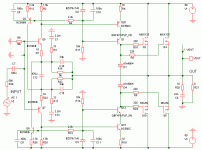
[edit] the driver stage on your schematic is not the same than mine (zeners and pot to tune the quiescent)
Last edited:
.
~300µa in the first stage, ~10ma in the driver,
Theses two numbers dont correlate at all when looking at the schematic.
If the input stage current is 300uA then you will have
1.4K x 0.0003A = 0.42V biasing voltage trough the 1.4K resistors
connected in the input stage collectors.
How this 0.42V , that is the biaising voltage of the VAS common
emitter , can yield 100mV through the 10R emitter resistors
since a transistor has 0.65V Vbe..??....
In my sims the input stage current is 356uA , i increased the 1.4K
resistors to 1.5K wich will slightly increase the VAS current but
not enough to have it properly working in class A.
Indeed , just doing the maths mentaly rapidly suggest theses
defects.
The value i gave where from the VFB( original amp) simulation. where the value of R5 was 6.8K
On my CFB sim, i have 600µa across the R5 1.4k, means 68,55V on the Q7 base, and 69,27V on the emitter. VBE is correct.
With 69.39-69.27 = 120 mv and 12mv at the sides of the R12 10ohms, everything looks perfectly coherent.
ps: i tried on my sims to get the current as close as possible on the VAS, for fair comparison. In real life, as i said, i have optimized my CFB amp for best results...
Last edited:
- Status
- This old topic is closed. If you want to reopen this topic, contact a moderator using the "Report Post" button.
- Home
- Amplifiers
- Solid State
- Is the CFB topology superior, and why?