Hello all,
Time has come that I've completed my amplifier design into a schematic that can reliably be built! All of the concepts turn out really well in the final design. The design went through multiple phases of which you can read all about in the thread "State-Of-MOS": 200W Ultra Low Distortion Pure FET Amplifier, along with various posts describing its workings.
This amp uses a radically new "VAS". The reason I'm quoting that word VAS is because of the fact that the stage is now actually two separate stages that are highly tied together. However, this yields enormous benefits in so many areas that this new "VAS" stage I developed, significantly improves performance over both a conventional single ended VAS and symmetrical VAS. I'm rather excited about it and to put it to a real test. But that will be one of the following steps to take; to design the PCB, build it and then measure and listen it.
This thread will also become the build log as this is the final design as I'm going to build it. Just shoot if you have any questions or have anything positive to add")
But for now, I will introduce to you MF500, an amp with (for now in the simulator) exceptional distortion and TIM figures; thank you for your time..
Time has come that I've completed my amplifier design into a schematic that can reliably be built! All of the concepts turn out really well in the final design. The design went through multiple phases of which you can read all about in the thread "State-Of-MOS": 200W Ultra Low Distortion Pure FET Amplifier, along with various posts describing its workings.
This amp uses a radically new "VAS". The reason I'm quoting that word VAS is because of the fact that the stage is now actually two separate stages that are highly tied together. However, this yields enormous benefits in so many areas that this new "VAS" stage I developed, significantly improves performance over both a conventional single ended VAS and symmetrical VAS. I'm rather excited about it and to put it to a real test. But that will be one of the following steps to take; to design the PCB, build it and then measure and listen it.
This thread will also become the build log as this is the final design as I'm going to build it. Just shoot if you have any questions or have anything positive to add
But for now, I will introduce to you MF500, an amp with (for now in the simulator) exceptional distortion and TIM figures; thank you for your time..
Attachments
Last edited:
Hi mj777,
I'm hoping it won't take too long to get started on PCBs. Right now I'm still doing some last minute changes, most notably having added the required opamp input stage due to the rather low input impedance of the amp itself. In the simulation I picked an NE5543AP which has offset inputs that can be used to trim the amp output. Overall distortion numbers don't change as this opamp has a huge bandwith still at unity gain.
The other change is to put an image together of a magnified view of the schematic but I'll have to make several screens and glue them together for that to obtain a hi-res image. It'll be up in the main post soon

No! They are deflectors! Photon deflectors! To protect the Warp Core in the back don't you see? Oh wait...
Yes, I'm going for this big power version right away; the sim already took me to the proof of concept comparing its relative performance to all kinds of (conventional) topologies so I am very confident about the outcome, this amp certainly won't blow up in your face and trample your music like it is a ripe grape
The mirrors are prominent to the design yes, it's what makes the concept work. The cascoded mirrors perform a number of tasks:
-Voltage domain conversion (fixed 30/30 at the IPS, 100/100 VCS for this design)
-Decoupling control voltage from the output voltage; output voltage is the signal swing, the input voltages can be anywhere between 30/30 theoretically.
-Sets a low gain input/output current ratio of 7 which results in:
-Strong outputvoltage rail current of 45mA
-Proportional input currents decoupled from any absolute voltage
-Power balancing between input/output current, most of the power goes into driving the output rather than wasting half of the power in the input rail with a 1:1 mirror otherwise
-Input currents drop in favourable range for the 4 gain devices that modulate the input currents.
-The 4-transistor gain unit can now be referenced against any voltage, in the design it is voltage centered in the middle of the IPS output voltage range.
There are more details, but these are the prime functions that the mirros perform on both sides. The whole stage operates in a 'current mode' of thinking
---------------------------merely curious, I didn't follow the development thread (I think that is what it is) and am not an expert on my next question. But, with the current mirrors providing "gain" are you depending on their linearity, or feedback to correct their linearity?
_-_-bear
Hi Bear, thanks for asking. No extreme linearity is required, the gain by parallelling the output devices in the mirror is merely to control the relation between the input/output current. This relation by nature is more lineair than a voltage controlled Vgs/Id slope. The task of the mirrors are not to provide the actual gain, that's left to the 4 devices in each mirror input rail. Hence the mirrors are easy to drive with a low current and still have a powerful voltage output rail, with a rather lineair relation between them two.
P.S. I looked at your website, you are a good man
Last edited:
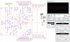
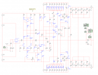
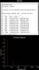
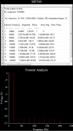
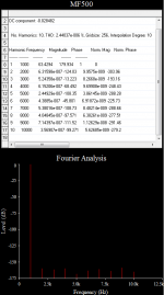
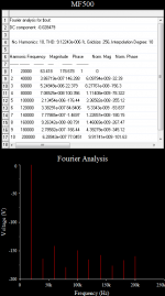
Well, I managed to put a good quality (I think) schematic image together now, you may have to scroll some. I also took some time to log some of the measurements from this amp. They are:
-THD1K 1W
-THD20K 1W
-THD1K Full Power
-THD20K Full Power
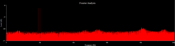
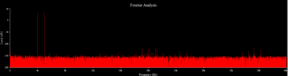
-TIM spectrum analysis 19K/20K with 50Hz resolution
-TIM spectrum analysis 4K/5K with 20Hz resolution
These numbers oughtta back up the schematic a bit When I find some time I think I will write a detailed description to the workings of the whole circuit, there's quite some thought behind it along with the compromizes (such as why 7 mirror transistors) to make things work at this power scale.
For now I'm qurious whether folks realize only half of what what this topology accomplishes other than being a trunk of trannies together
Edit: I did not connect the opamp null offset; this particular model did not match the datasheet on pin out so I just left it. You can basically pick any decent opamp frontend, but this NE5534 works well, amongst the best I've tested in the sim. It can cope with the required 10mA full signal drive and you could even apply Douglas Self's opamp parallelling here because they are configured as unity gain buffers whose outputs are then simply summed into the J-FET virtual ground node. All you need to do is to divide the input impedance resistor by the number of opamps you'll use. In the schematic, if you'd parallel two 5532's you'd use an output resistor of 200 Ohms per opamp. It makes the life of the opamps twice as easy. In this case this would be applied to share the relatively high drive current of the amp input.
-THD1K 1W
-THD20K 1W
-THD1K Full Power
-THD20K Full Power
-TIM spectrum analysis 19K/20K with 50Hz resolution
-TIM spectrum analysis 4K/5K with 20Hz resolution
These numbers oughtta back up the schematic a bit
When I find some time I think I will write a detailed description to the workings of the whole circuit, there's quite some thought behind it along with the compromizes (such as why 7 mirror transistors) to make things work at this power scale.For now I'm qurious whether folks realize only half of what what this topology accomplishes other than being a trunk of trannies together
Edit: I did not connect the opamp null offset; this particular model did not match the datasheet on pin out so I just left it. You can basically pick any decent opamp frontend, but this NE5534 works well, amongst the best I've tested in the sim. It can cope with the required 10mA full signal drive and you could even apply Douglas Self's opamp parallelling here because they are configured as unity gain buffers whose outputs are then simply summed into the J-FET virtual ground node. All you need to do is to divide the input impedance resistor by the number of opamps you'll use. In the schematic, if you'd parallel two 5532's you'd use an output resistor of 200 Ohms per opamp. It makes the life of the opamps twice as easy. In this case this would be applied to share the relatively high drive current of the amp input.
Attachments
Last edited:
MagicBox, why not save the schematic as a PDF, then it can be viewed any size the reader wants also save it for later reference.
I take it that your aim was to lower the total noise in the bunch of parallel sources by root 8 due to the summing of non-coherent noises else you would have used single devices, correct?
Interesting design my friend, a little complex but clever.
I take it that your aim was to lower the total noise in the bunch of parallel sources by root 8 due to the summing of non-coherent noises else you would have used single devices, correct?
Interesting design my friend, a little complex but clever.
Last edited:
Hi Nico
Did you mean the sources of the output transistors or the ones in the current mirrors? I assume that you mean the transistors in the currentmirror, though. I'd say no, I didn't choose multiple transistors to reduce noise, although if that is a side results, that's just another free benefit
I did it because I primarily wanted to mirror the full swing vas rail so I would have a second rail whose voltages I could divide freely, thus being able to position the gain/bias element anywhere between supply rails. With a small scale amp, a 1:1 mirror would probably be sufficient.
This amp however sports 200V across its voltage output rail and to maintain a high bandwidth the quiesent current through this VAS rail is relatively high, chosen at 45mA. If it were 50mA, the rail as a whole would dissipate 10 watts. That current mirrorred 1:1 would still be 45mA. A quite high current for the gain devices and another 10 watts of dissipation doing nothing but accepting controlling currents within a free-to-pick voltage range. So, that's why I added the devices, to explicitly make use of the current multiplication property that the Wilson Mirror provides and 'move' current from the mirror input to the output. With a control input of 6.43mA quiesent current into both legs that amounts to 51.43 mA which is a little over 10 watts of dissipation, barely a bit more than the power I need to drive the output stage.
Because the mirror itself is not supposed to act as a current gain stage, the multiplication shouldn't be too high either. Just high enough to balance the input and output rail currents so that most of the dissipation goes into the VAS output rail. Then we have the practical number of transistors, thus multiplication factor and boardspace to consider, which together made me strike a compromize at a factor of 7 for a total of 8 transistors per mirror.
Oh as for turning the schematic into a PDF, I'll do that when I am going to draw the schematic into PCAD for PCB development and output to PDF from there, then the supplies and other sub schematics will end up in there too. For now you could save the schematic image at the bottom of the first page or rightclick it and "View link in another tab". That will show the image directly into your browser and you can then zoom in/out and scroll.
I hope it makes sense what I say.. if not just say so, I'm open to positive critics
Last edited:
Hi,
I've now started to breadboard pieces of the concept and after initial troubles (the high bandwith current test source) and so far it works out well. Cascodes and a reasonable matching are required for the mirror elements, but they'll do the job perfectly. Once I've scaled it up to 7 mirror devices and completed the whole circuit I'll try to run an AC analysis on it.
I've now started to breadboard pieces of the concept and after initial troubles (the high bandwith current test source) and so far it works out well. Cascodes and a reasonable matching are required for the mirror elements, but they'll do the job perfectly. Once I've scaled it up to 7 mirror devices and completed the whole circuit I'll try to run an AC analysis on it.
I've cascoded the output with an IRF9510 picking a zener that causes the exact same voltage drop over the mirror output Vds as the input Vds (= Vgs average of whole mirror block). This one I 'silenced' with a local feedback cap of 22pF. All the mirror transistors have their gates directly connected, no resistor in between. This just degrades performance. A mirror is a pure slave topology with a high bandwidth, if you stabilize the input, the output will follow provided the gates are indeed as directly connected as possible to reduce lag/oscillation in the output response. I knew when things where oscillating on my test setup without even attaching a scope only 2 well placed 22pF ceramics were needed to get it all stable. I'm using 12Ohm degenerative resistors in the source leads btw with a 5mA current per mirror transistor.
Under the cascoded configuration with the equal Vds voltages it's easy to match them and once a good match is made, the mirror is surprisingly stable with temperature.
only 2 well placed 22pF ceramics were needed to get it all stable. I'm using 12Ohm degenerative resistors in the source leads btw with a 5mA current per mirror transistor.Under the cascoded configuration with the equal Vds voltages it's easy to match them and once a good match is made, the mirror is surprisingly stable with temperature.
Last edited:
No prolblem.. I meanwhile extended the number of transistors to 4 and still have an exact gain of 4 and that worked too, being stable without any compensation other than the 22pf local feedback on the current source output transistor, a BC550C and one across the opamp output/negative input. There is a reasonable amount of current swing possible without the multiplier drifting much. The more curves are matched, the more this drifting is minimized. Within +/-10% of the qiescent current the multiplier barely changes. The accuracy of the multiplier matters only to the DC bias for the construction, and that's as accurate as your match on the intended current. S far it's all going well and I'm expecting the breadboard version of the input- and driver stage to work as intended, at least, as a functioning negative feedback amplifier
I meanwhile extended the number of transistors to 4 and still have an exact gain of 4 and that worked too, being stable without any compensation other than the 22pf local feedback on the current source output transistor, a BC550C and one across the opamp output/negative input. There is a reasonable amount of current swing possible without the multiplier drifting much. The more curves are matched, the more this drifting is minimized. Within +/-10% of the qiescent current the multiplier barely changes. The accuracy of the multiplier matters only to the DC bias for the construction, and that's as accurate as your match on the intended current. S far it's all going well and I'm expecting the breadboard version of the input- and driver stage to work as intended, at least, as a functioning negative feedback amplifier
Last edited:
Things going well I've got about 100 each of BS170 and BS250. I've been able to match an 8-transistor P mirror with the BS250's under +-2mV GS difference at the intended operating current, temperature and tension, the result is sweet! I have to match some more and meanwhile wait for an order of a 610/9610 batch, 2SK170's and assorted JFETs for the current sources. But it should then be possible to build an operational front/mid end..
I've got about 100 each of BS170 and BS250. I've been able to match an 8-transistor P mirror with the BS250's under +-2mV GS difference at the intended operating current, temperature and tension, the result is sweet! I have to match some more and meanwhile wait for an order of a 610/9610 batch, 2SK170's and assorted JFETs for the current sources. But it should then be possible to build an operational front/mid end..
Last edited:
Dear Mirror, dear Mirror, who's the most gorgeous man...
Oh wait.. I think I can say I finished the north side BS250 mirror 8 Transistors, 8 12 Ohm degen resistors cascoded and all with an input current of 6.43, which gives an approximate current of 45mA. The current stays reasonably stable with temperature. All gates are directly connected; the degens function as NFB too besides averaging out the remaining Vgs differences and lessening their impact some more. Bandwith exceeds 2MHz easily, the current source into which I injected a 2MHz test signal suffered severe rolloff, but modulating right into the mirror let it through full power. The mirror has at least 20mA lineair swing too, it's great. Together with accurate and secure assembly, this is going to be a great building block for this amp
Oh wait.. I think I can say I finished the north side BS250 mirror
8 Transistors, 8 12 Ohm degen resistors cascoded and all with an input current of 6.43, which gives an approximate current of 45mA. The current stays reasonably stable with temperature. All gates are directly connected; the degens function as NFB too besides averaging out the remaining Vgs differences and lessening their impact some more. Bandwith exceeds 2MHz easily, the current source into which I injected a 2MHz test signal suffered severe rolloff, but modulating right into the mirror let it through full power. The mirror has at least 20mA lineair swing too, it's great. Together with accurate and secure assembly, this is going to be a great building block for this amp - Status
- This old topic is closed. If you want to reopen this topic, contact a moderator using the "Report Post" button.
- Home
- Amplifiers
- Solid State
- MF500 | My 500W/4Ω Hi-Fi All-FET Amp Design