Dear Mirror, dear Mirror, who's the most gorgeous man...
Now if you were an Italian.....
LOL gotta give those credits to them yes 
Those BS170's are much closer together in differences, they're much easier to match. I've also found a way to now autiobias by outputcurrent, rather than by inputcurrent, which means that any minor drifting in the mirrors is compensated for which means you'll get a rock solid VAS DC current to bias the output stage with
Those BS170's are much closer together in differences, they're much easier to match. I've also found a way to now autiobias by outputcurrent, rather than by inputcurrent, which means that any minor drifting in the mirrors is compensated for which means you'll get a rock solid VAS DC current to bias the output stage with
Well, finally got around to order a reasonable number of assorted transistors. J111, J112, J113, BF245B, 2SK170GR, IRF610, IRF9610, BC547C, BC557C. That should give me enough to play with and continue the design
I already had it somewhat stable, but the stability issue came from the biassing circuit which was not worked out very well in the initial design. Now that I am measuring the VAS output current I had to change around the biascontroller and a week ago I made that part into a final version that works great. It exhibits a controlled startup. No chicken/egg problems or otherwise potential latching. Once I get those ordered transistors I'll be able to build and test it.
From that moment and on I should be able to get going the VAS properly
Hi guys
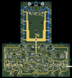
It's been a bit silent around my project but recently I had time to casually build the final schematic and PCB design. It's been designed for mounting it to a 25cm (Height) x 30cm (Depth) at a minimum. I will be using 25cm x 40cm heat sinks. There's still an open space at the upper part which is reserved for the DC error detector. The bits that already sit up there is a clip detector.
Everything's been sorted out, from the autobiassing VAS to a DC offset servo. The LTP current can also be finetuned. Further the design contains an integrated pre-input stage that uses an INA137 to take a balanced input and buffer it to drive the low impedance LTP inputs which are as low as 100 Ohms. I think the PCB turned out really nice. The ground plane functions as the ideal star for well.. the ground. There are very few lines drawn at the bottom layer so there's no obstruction of major ground returns.
Some of these days I'll start collecting the components required before I have the PCB made, but for now you can see the project is not dead
Attachments
I'm surprised there are no comments, be them good or bad =)
P.S. The final schematic has all the appropriate components that might be missing in individual simulation schematics. I expect this PCB to work for 95% with some 5% fine tuning left (ugly rewires/removals of components etc).
P.S. The final schematic has all the appropriate components that might be missing in individual simulation schematics. I expect this PCB to work for 95% with some 5% fine tuning left (ugly rewires/removals of components etc).
Last edited:
lol thanks! It may look a bit odd, no degens for the output transistors, but it'll be ECX10N20 and ECX10P20 being parallelled and used, they can do without them and should improve output impedance and overall output accuracy.
What would one consider for a DC protection, keeping SQ in mind:
-Regular relais that disconnects, or..
-TRIAC crowbar to blow fuses?
What would one consider for a DC protection, keeping SQ in mind:
-Regular relais that disconnects, or..
-TRIAC crowbar to blow fuses?
Getting into the triple zeros with distortion is massively dependant on layout.
Hi Boscoe, that's a suggestive remark; would you have anything more tangible to say?
I prototyped the layout (T-shape with opposite transistors and an unobstructed ground plane) with my MF80 design, and taking out the noise floor it measured around 0.000117 THD (see 10KHz FFT of MF80; the worse distortion at the lower freqs was due to a too low value feedback cap. This was measured with a PC/soundcard setup, hence the noise floor.
So, I'm very confident about the layout; it's the actual circuit design that will be the exciting part
Will it work as intended or will I end up with smoke? We'll see..Regardless, feel free to tell any hints that I might incorporate to end up with a better design.
Hi Boscoe, that's a suggestive remark; would you have anything more tangible to say?
I prototyped the layout (T-shape with opposite transistors and an unobstructed ground plane) with my MF80 design, and taking out the noise floor it measured around 0.000117 THD (see 10KHz FFT of MF80; the worse distortion at the lower freqs was due to a too low value feedback cap. This was measured with a PC/soundcard setup, hence the noise floor.
So, I'm very confident about the layout; it's the actual circuit design that will be the exciting part
Regardless, feel free to tell any hints that I might incorporate to end up with a better design.
Sorry no I was unable to view the layout I posted because of my phone. It looks good however. You might be better off with 4 layers for an amp of this potential and complexity?
I think that's goung to be quite expensive, I'll have to figure out costs first. Besides, I made a few more modifications removing more bottomside copper. Right now I'm going to focus on the case and the output power supply which is huge. I gotta find me a cheaper PCB factory too Eurocircuits is good but very expensive.
Eurocircuits is good but very expensive.- Status
- This old topic is closed. If you want to reopen this topic, contact a moderator using the "Report Post" button.
- Home
- Amplifiers
- Solid State
- MF500 | My 500W/4Ω Hi-Fi All-FET Amp Design