I am facing (for hobby) the design of an output only stage. The front end (including the VAS) is unfortunately single-ended outoput , so there is no provision for the return path of the bias spreader and its power supply is not available externally.
The front end power supply voltage is larger that the output stage one in order to ensure rail-to-rail swing and has a Ro of 33 Ohm.
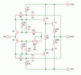
The problem is how to implement an adjustable bias spreader in the output stage also in order to compensate for thermal drift. I have scketched here a possible solution, but it looks "hairy" to me. Some hints?
Thanks in advance
The front end power supply voltage is larger that the output stage one in order to ensure rail-to-rail swing and has a Ro of 33 Ohm.
The problem is how to implement an adjustable bias spreader in the output stage also in order to compensate for thermal drift. I have scketched here a possible solution, but it looks "hairy" to me. Some hints?
Thanks in advance
Attachments
I am facing (for hobby) the design of an output only stage. The front end (including the VAS) is unfortunately single-ended outoput , so there is no provision for the return path of the bias spreader and its power supply is not available externally.
The front end power supply voltage is larger that the output stage one in order to ensure rail-to-rail swing and has a Ro of 33 Ohm.
The problem is how to implement an adjustable bias spreader in the output stage also in order to compensate for thermal drift. I have scketched here a possible solution, but it looks "hairy" to me. Some hints?
Thanks in advance
Yes that's hairy
")
But why not use two 'normal' bias spreaders in series with the mid point driven?
The amplified diode topology?
I've used that on occasion and it works as it should.
jan didden
That is what it should be in the drrawing.Yes that's hairy
But why not use two 'normal' bias spreaders in series with the mid point driven?
What is that?The amplified diode topology?
R1’s way too large. Should be something like 20 ohms. C1’s pretty pointless and may produce some oddities if you bother to check the FFT. If you feel more comfortable using it then at least drop it to .047uF. Q6 & Q4 should be mounted to the output heatsink (the drivers need some good heatsinking too). In the bias spreader scheme return R4 to the collector of Q6 and R5 to the collector of Q4 instead of the rails. Pots should be around 2K 20 turn, and will be a PITA to adjust. Power supply rejection could be an issue due to R6 & R7 connecting to the +/- 30V rails (these rails ideally need to be solid if you use this scheme). If the driver stage can indeed approach its 40 volt rails then you could end up reverse biasing and breaking down Q6 & Q4 resulting in parametric shifts to these devices.
R1’s way too large. Should be something like 20 ohms. C1’s pretty pointless and may produce some oddities if you bother to check the FFT. If you feel more comfortable using it then at least drop it to .047uF. Q6 & Q4 should be mounted to the output heatsink (the drivers need some good heatsinking too). In the bias spreader scheme return R4 to the collector of Q6 and R5 to the collector of Q4 instead of the rails. Pots should be around 2K 20 turn, and will be a PITA to adjust. Power supply rejection could be an issue due to R6 & R7 connecting to the +/- 30V rails (these rails ideally need to be solid if you use this scheme). If the driver stage can indeed approach its 40 volt rails then you could end up reverse biasing and breaking down Q6 & Q4 resulting in parametric shifts to these devices.
Those are the minor secondary points. The problem is that the bias speader has a large gain with this transistor topology and will not worlk reliably whatever R1, C1 etc.
He needs to put in two 'regular' amplified diodes (and Hawksford's topology is already too advanced, forget it for the moment). Look at any push-pull amp with a Vas stage, copy the bias spreader two in series and drive from the center. In fact, unless you have no global feedback, there's no need for two trimpots, one is enough in one of the spreaders. Done.
THEN you can start to fight about details like R1, C1 etc.
jan didden
Hmm, don’t think you bothered to read my post accurately. Changing R4 and R5 to the collectors of Q6 & Q4 does make them standard Vbe multipliers. R6 & R7 do need to be changed to much higher values though, or everything’s going to fry. But you are right about the number of spreaders, if the previous stages are happy being offset and global feedback is unity at DC then only one spreader is necessary.
Thanks, that was my mistake! The rest of the amplifier I have just thrown in, so much for R1 & C1. The OP in reality will be many paralleled and there will be huge h/s.. In the bias spreader scheme return R4 to the collector of Q6 and R5 to the collector of Q4 instead of the rails. .
And yes, the spreader will be defenetly reverse biased with the larger signals. Would it make sense to put a godd 1n4007 diode in series with Q6 & Q4 emitters?
Yes, the intend value would be 4.7 K sorry. In reality the drive current will come almost all from the F.E. that is able to supply a couple of A.R6 and R7 need to be much higher resistance, and should be bootstrapped. As it is, the bias transistors (Q4 and Q6) have to conduct about 700mA, and the front end is driving a load of about 23 Ohms.
Can you elaborate on "bootstrapping" R6 and R7? Why'? (i.e. in order to ensure max swing) . How?
Thanks Jan. Intersting article.This should cover it.............
It look like something D. Self calls somehow magic resistor.
It does not add so much complication, however, in my opinion.
That's elegant!If there's no need to adjust DC offset, then only one trimmer is needed, as in the circuit below. C1 and C4 are debatable. I just included them to show an alternative to the cap in the original schematic.
And why you say you can't adjust? It looks like that you can't just adjust the bias SIMMETRICALLY . But, even done asimmerically global feeback will take care of that, I hope.
Hmm, don’t think you bothered to read my post accurately. Changing R4 and R5 to the collectors of Q6 & Q4 does make them standard Vbe multipliers. .
Yes I missed that, apologies.
That was also my point.
jan
In the circuit I showed in post 9, C2 and C3 provide the bootstrap. The output drives R7 and R10 through the capacitors, so the voltage across R8 and R9 is almost constant.Can you elaborate on "bootstrapping" R6 and R7? Why'? (i.e. in order to ensure max swing) . How?
- Status
- This old topic is closed. If you want to reopen this topic, contact a moderator using the "Report Post" button.
- Home
- Amplifiers
- Solid State
- Bias speader for single ended front end