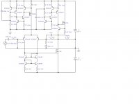
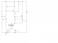
This is my new design of a two stage pure class A amplifier. Output power is 5,1 Wpc into 12 ohms for input of 2 V RMS (10,2 W in stereo). Z input is 5k9 aprox.
Very simple design...
Output in single ended...
Zero hum...
Zero hiss...
Excellent linearity...
Ultra fixed bias...
Ultra high PSRR...
Ultra high dinamics...
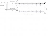
A stereo system requires four power transformers...
A lot of headroom and the most important: musical and perfect sound...
PD: in the schematics 4700,1 uF = 4700 uF electrolitic capacitor plus 100 nF ceramic capacitor.
Very simple design...
Output in single ended...
Zero hum...
Zero hiss...
Excellent linearity...
Ultra fixed bias...
Ultra high PSRR...
Ultra high dinamics...
A stereo system requires four power transformers...
A lot of headroom and the most important: musical and perfect sound...
PD: in the schematics 4700,1 uF = 4700 uF electrolitic capacitor plus 100 nF ceramic capacitor.
Attachments
Last edited:
A few suggestions...
Power supply should be C-R-C-C-Cfm. Decoupling and proper grounding is very important. Those large mosfets will need a lower impedance gate drive for sure. This includes the CCS on the top half, and the amplifier on the bottom half. The CCS for the differential tail current is way over-complicated. The LTP needs some emitter degeneration. Consider ditching the IRF9610 for a less noisy component like a BJT. The CCS driving the output CCS is too complicated too, also 0.6V/33K=18uA bias?
Power supply should be C-R-C-C-Cfm. Decoupling and proper grounding is very important. Those large mosfets will need a lower impedance gate drive for sure. This includes the CCS on the top half, and the amplifier on the bottom half. The CCS for the differential tail current is way over-complicated. The LTP needs some emitter degeneration. Consider ditching the IRF9610 for a less noisy component like a BJT. The CCS driving the output CCS is too complicated too, also 0.6V/33K=18uA bias?
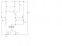
On the three CCS used for each of the two CCS , one can be removed
for each without changing the PSRR by a iota.....
The 4700.1 uF capacitors are not a good idea , particularly the one
on the differential s CCS , as it increase hugely the amp s settling
time at power on , and given the lower resistors values attached to
the output stage CCS cap , it may well be that it will be functional
before the one of the input stage , hence , the former may send an
impulse to the speaker at full rail voltage at power on....
The CCS (output) gets zero current variation (considering three decimal places, eg 1.128 Acc) for a variation of output voltage excursion between + - 11.08 volts peak and between a variation of positive supply voltage between 4.9 and 37.1 volts. This is laboratory tested.
0.6 V / 33 K = 18 uA (may be close to that, but it's no problem). There is no reason to worry. Try it if you want if you have questions.
The CCS (input) gets zero current variation (considering two decimal places, eg 8.67 mA) for a variation of positive supply voltage between 4.9 and 37.1 volts. This is laboratory tested, too. The variation of the signal excursion present there is rather low, therefore does not influence too.
With respect to the first connection, no plop in speaker!. Total silence. Believe it!.
Degeneration could be implemented in the LTP, yes. You can try, if you wish. Would improve the linearity even more than is actually obtained.
Try it with full confidence, it will not be disappointed. I have it running for over a year. The sound I get with my speakers is outstanding.
regards
Last edited:
I think is too high resistor of 820 ohms from VAS constant current source.
For example, if total gate charge for IRF150 is max. 125nC, then instantaneous peak current required when the gate will be:
I = k * (125E-9 * f) = 100 * (125E-9 * 50,000) = 0.625A.
where:
k = headroom factor for accurately reproducing a square/rectangular wave (especially at high frequencies);
f = maximum frequency that needs to be reproduced correctly (in the example above we chose 50 kHz, a typical value for the calculation of audio amplifiers)
So, it's good to polarized VAS at least 0.625/2 = 0.3125 A. Do not forget to design a class A amplifier, so, that resistance of 820 ohms will be:
R = 0,65V/0,3125A = 2 Ohm.
But here there is still a problem. It may not be properly included in amplifier topology the IRF150 from the negative voltage source. Here you must include pre-driver transistor.
So, more must be put scheme, tested practice, calculated and tested, to obtain high throughput.
I think is too high resistor of 820 ohms from VAS constant current source.
For example, if total gate charge for IRF150 is max. 125nC, then instantaneous peak current required when the gate will be:
I = k * (125E-9 * f) = 100 * (125E-9 * 50,000) = 0.625A.
where:
k = headroom factor for accurately reproducing a square/rectangular wave (especially at high frequencies);
f = maximum frequency that needs to be reproduced correctly (in the example above we chose 50 kHz, a typical value for the calculation of audio amplifiers)
So, it's good to polarized VAS at least 0.625/2 = 0.3125 A. Do not forget to design a class A amplifier, so, that resistance of 820 ohms will be:
R = 0,65V/0,3125A = 2 Ohm.
But here there is still a problem. It may not be properly included in amplifier topology the IRF150 from the negative voltage source. Here you must include pre-driver transistor.
So, more must be put scheme, tested practice, calculated and tested, to obtain high throughput.
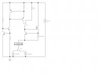
I do not understand why you associated only to the 820 ohm resistor as the only fixed the polarization of the output bias. The entire constant current source is composed of six transistors and other components (at the top right of the circuit)!.
Suppose that the electric charge of the gate of the IRF150 is as you say, once loaded, shortly after connecting the amplifier, the current to the collector of the BC550 (associated with IRF150 in the top of the diagram) remains constant linearizing their performance (controlling the upper MOSFET). In this way it controls much more efficient to IRF150.
If I employ two identical resistors (plus the bootstrap capacitor, as is seen in the Aleph, for example) to bias the gate of the IRF150 and the collector of the BC550, the current through the collector of the BC550 will vary widely depending upon how it varies the output signal of the amplifier.
regards
Last edited:
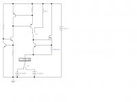
This is a brief comparison between tradicional CCS and my CCS design.
Reducing the 66K resistor (in the example), the effect of variation in bias current between the peaks of the output signal is maximized.
It is understood that the resistance of 66K is split into two 33K (plus the bootstrap capacitor, that was not put in the scheme).
regards
Reducing the 66K resistor (in the example), the effect of variation in bias current between the peaks of the output signal is maximized.
It is understood that the resistance of 66K is split into two 33K (plus the bootstrap capacitor, that was not put in the scheme).
regards
Attachments
Last edited:
To explain in more detail what I meant in previous post. Was well if you numbered electronic components in the amplifier diagrams.
So, the top MOSFET, the positive supply side, is a constant current source for the bottom MOSFET will work in class A. But both, above and below, where the intended use of less than 12 ohm impedance on the output MOSFET is not enough one, but you have to use several MOSFET's in parallel. So you have to keep in mind and this.
You amplifier diagram have a supply voltage of 32.7 Vdc per branch or +/-32.7Vdc. For audio amplifier to work perfectly in class A, he need be biased to half the peak current on the lowest impedance supported. For example, if we assume minimum output impedance admitted to be equal to 4 ohms, the peak current would be I_peak = 32.7 V/4 Ohm = 8.175 A. Polarization current in class A will be a maximum of 8.175 / 2 = 4.08A. So, in this case if yo u take the minimum load of 4 ohms, you should use several MOSFET's in parallel. In fact, if you resume the calculations, you will notice that: for 8 ohms and you need more MOSFET's in parallel for a safe operation.
So, if for 4 ohms you need a 4A bias current, then for 8 ohms, you need a bias current about 2A (therefore, approximately).
Now, let's look polarization or current needs of the both IRF150 gate's. In this respect we look at the IRF150 datasheet, see the drain current transfer characteristic = f (voltage U_GS). According to the features you need about 5V on the mosfet grid to have a bias current of 4A sau for 8 Ohm load you need 4.75V.
The source above IRF150 there 0.56Ohm resistance. Let's see if calculated correctly.
R = 0.65V / 4.08A = 0.159 Ohm (so, is wrong 0.56 Ohm);
R = 0.65V / 2.00A = 0.320 Ohm (so, is wrong 0.56 Ohm);
I see now you choose 12 Ohm load, that mean bias current about: 1.36A, then result:
R = 0.65V / 1.36A = 0.470 Ohm (so, is wrong 0.56 Ohm);
Potential difference between terminals C and E bipolar transistor located near IRF150 transistor from the positive supply side, it should be about 5V. Between terminals C and E would mount a capacitor whose capacity we calculate later. It is helpful to mount the capacitor to avoid the polarization grid MOSFET with excessive bias current (so as not to reach those 0,3125A that I calculated in the previous post). It's a tactic that is practiced in class AB amplifiers with vertical FET's. So, will provide additional capacitor mounted part of the required peak current gate MOSFETs. If we do that, then we replace that with a resistance of 820 ohms resistance up to three times smaller but not with the value 2 Ohms.
Capacitor calculation - that capacitor will have to provide approx. 66% of peak current on the gate MOSFETs.
C = (0.66 x Q) / U = 0.66 x 125E-9 / 5 = 16.5 nF (you can choose standard capacitor, for example 10nF or 22nF). This capacitor will have to be found and between grid and source other MOSFET.
Currently going to stop here, a lot to say and ... simulated / practicable, to obtain a quality class A audio amplifier.
Last edited:
The top mosfet is a CCS and so being a single end class A amplifier, CCS bias would be set at the peak output current. For a 12R speaker, it is reasonable to assume that worst case scenario is that dynamic Z could be 1/2 of that, so at 6R load bias would be 5.5A. This would require at least 2 parallel devices to remain in safe SOA at 33V, perhaps 3. Even for 8R, bias would be 4.1A and taking into account derating, 2 devices would be required for safe SOA. Since this is a CCS, once Vgs for this conductance is established it would remain constant so the charge for Cgs would not need to be changed and so the 'driver' current could be small with regard to this circumstance. However, Cgd would be an issue when the device approaches Vds saturation at peak signal and would become a nasty dynamic impedance thrown onto the CCS 'driver'. The initial charging of Vgs would have a time constant so a smaller charging current would result in a larger time delay of conductance at start up, requiring the differential to make the difference in the bottom mosfet to suit the 0VDC initial output condition. I suggest a larger 'driver' current for the top mosfet CCS or limit the output voltage to not approach clipping. I believe Mr Pass mentions this at the behest of those who blast him for a larger lack of effeciency. But then it is a single end class A amplifier so obviously efficiency is not a priority.")
The bottom mosfet is the amplifier and would show a dynamic impedance related to both Cgs and Cgd. This would require a much lower driver impedance to properly handle this load. The 4mA of current (1/2 of the tail current from input differential) would not be enough to handle this dynamic load. A driver stage buffer should be employed. Also I see no local compensation for the mosfets. I would suggest in addition to gate stopper resistors, employing gate to drain Zobel filters, IOW using a zero to dampen the oscillator that is formed with, in particularly power mosfets, between the internal capacitances and the lead inductances. This should be done right at the device package. These being TO-3 devices, keep in mind that any wires attached directly to the devices become lead inductors. I hope these suggestions don't come off as condescending, but more to constructive criticism. Power mosfets, particularly vertical type, when used as analog devices can be somewhat irksome when it comes to stability.
The bottom mosfet is the amplifier and would show a dynamic impedance related to both Cgs and Cgd. This would require a much lower driver impedance to properly handle this load. The 4mA of current (1/2 of the tail current from input differential) would not be enough to handle this dynamic load. A driver stage buffer should be employed. Also I see no local compensation for the mosfets. I would suggest in addition to gate stopper resistors, employing gate to drain Zobel filters, IOW using a zero to dampen the oscillator that is formed with, in particularly power mosfets, between the internal capacitances and the lead inductances. This should be done right at the device package. These being TO-3 devices, keep in mind that any wires attached directly to the devices become lead inductors. I hope these suggestions don't come off as condescending, but more to constructive criticism. Power mosfets, particularly vertical type, when used as analog devices can be somewhat irksome when it comes to stability.
This is a brief comparison between tradicional CCS and my CCS design.
Reducing the 66K resistor (in the example), the effect of variation in bias current between the peaks of the output signal is maximized.
It is understood that the resistance of 66K is split into two 33K (plus the bootstrap capacitor, that was not put in the scheme).
To continue...
In all those all 4 diagrams, if you try to implement them in practice you will find the value output offset voltage is very high and... is not allowed.
I tried to implement a simulation below with your project, to see that there are many mistakes that should fix them.
Attachments
You amplifier diagram have a supply voltage of 32.7 Vdc per branch or +/-32.7Vdc. For audio amplifier to work perfectly in class A, he need be biased to half the peak current on the lowest impedance supported. For example, if we assume minimum output impedance admitted to be equal to 4 ohms, the peak current would be I_peak = 32.7 V/4 Ohm = 8.175 A. Polarization current in class A will be a maximum of 8.175 / 2 = 4.08A. So, in this case if yo u take the minimum load of 4 ohms, you should use several MOSFET's in parallel. In fact, if you resume the calculations, you will notice that: for 8 ohms and you need more MOSFET's in parallel for a safe operation.
So, if for 4 ohms you need a 4A bias current, then for 8 ohms, you need a bias current about 2A (therefore, approximately).
Now, let's look polarization or current needs of the both IRF150 gate's. In this respect we look at the IRF150 datasheet, see the drain current transfer characteristic = f (voltage U_GS). According to the features you need about 5V on the mosfet grid to have a bias current of 4A sau for 8 Ohm load you need 4.75V.
The source above IRF150 there 0.56Ohm resistance. Let's see if calculated correctly.
R = 0.65V / 4.08A = 0.159 Ohm (so, is wrong 0.56 Ohm);
R = 0.65V / 2.00A = 0.320 Ohm (so, is wrong 0.56 Ohm);
I see now you choose 12 Ohm load, that mean bias current about: 1.36A, then result:
R = 0.65V / 1.36A = 0.470 Ohm (so, is wrong 0.56 Ohm);
The maximum output excursion for which it was designed not is 32.7 volts (peak). The maximum output excursion was set at no more than 11.08 V approx. (peak). Then, as the impedance of the load I use never falls below 12 ohms, the maximum current peak is at most 0.923 A. If you look 0.65 V / 0.56 ohms = 1.161 A approx. (in my real case is 1.128 A).
I use a CD player with no more than 2 V RMS.
I do not see what is the problem with the output current. The amplifier was not designed to work below 12 ohms. Is the design pattern.
I use high output impedance instead of the traditional 2, 4, 6 or 8 ohms, because in this same way I get a wider dynamic range. I give an example, for every doubling of output impedance get about 6 dB higher range, using the same interconnect resistance. For example: With 16 ohms achieving a range around 24 dB higher than 2 ohms, changing only the voltage and current relationships!. I designed this amplifier to behave more appropriately in 12 ohms and low levels of distortion achieved mainly in the range of voices.
I can admit that it is necessary to add resistors (stopper) to those mosfet transistors, as well someone has suggested.
The output MOSFET work almost to the limit, it is true. But simulations showed different disadvantages of adding more pairs.
Do not think I have not run simulations. I've run a lot and I've even seen many differences with the actual operation. I have made many measurements, too. Do not think I present a circuit just like that.
I know very well what I can rely on simulations and know very well what I can trust the measurements.
Regards
Last edited:
- Status
- This old topic is closed. If you want to reopen this topic, contact a moderator using the "Report Post" button.
- Home
- Amplifiers
- Solid State
- PerfectA Mosfet Power Amp