Hi there!
I tried building an ESP P3A (for general amplification, I am not really chasing the "crystal clear sound") since I needed a 50-100W amplifier.
My current test runs involve 12V 21W incandescent bulbs in places of fuses and +-12V power supply (in practice this means 11.8V @ each supply rail). When the amp is powered up this way, the lamps do not even start glowing, therefore consumed current can't be too high. I have not measured that.
However, the output is constantly at 2.34V, therefore I have not risked hooking a speaker there. With 100 ohm dummy load it dropped to 2.28V, but am I mistaken if I believe it should not be more than 0.1-0.2V there without any load?
I have made some modifications:
1) readily-available transistors MJE3055 & MJE2955
2) currently 1 ohm resistors for output transistors (originally I tried with 0.1 ohm but replaced them with 1 ohm just to be sure this is not related to my issues)
3) BC547 instead of BC546
I have desoldered and measured every transistor individually, they all seem fine, therefore I am out of ideas where to look for the issues. I was hoping some kind person would check out my measurements and give me some directions where to look at to find my problems.
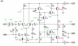
In the attached picture I marked any differences with original schematic with red and measured voltages in dark green.
I tried building an ESP P3A (for general amplification, I am not really chasing the "crystal clear sound") since I needed a 50-100W amplifier.
My current test runs involve 12V 21W incandescent bulbs in places of fuses and +-12V power supply (in practice this means 11.8V @ each supply rail). When the amp is powered up this way, the lamps do not even start glowing, therefore consumed current can't be too high. I have not measured that.
However, the output is constantly at 2.34V, therefore I have not risked hooking a speaker there. With 100 ohm dummy load it dropped to 2.28V, but am I mistaken if I believe it should not be more than 0.1-0.2V there without any load?
I have made some modifications:
1) readily-available transistors MJE3055 & MJE2955
2) currently 1 ohm resistors for output transistors (originally I tried with 0.1 ohm but replaced them with 1 ohm just to be sure this is not related to my issues)
3) BC547 instead of BC546
I have desoldered and measured every transistor individually, they all seem fine, therefore I am out of ideas where to look for the issues. I was hoping some kind person would check out my measurements and give me some directions where to look at to find my problems.
In the attached picture I marked any differences with original schematic with red and measured voltages in dark green.
Attachments
Weird, voltage across c1.... Make new measurements when you disconnect any input and short the point between r1 and r3 to gnd. BC547 should be fine. Have you used the bd139 and bd140's? Check the pinout of those parts. They might be different from the ones used in your pcb-layout-program. What is your bias "voltage"?
Last edited:
BD139 and BD140's certainly have the correct pinout. Since base is not the middle pin, I can easily identify pins with multimeter.
I will now proceed to short the point between R1 and R3 to ground and take new measurements.
EDIT: The results are in and I still can't make any sense of it.
EDIT2: I noticed you asked about my bias voltage. My trimpot is set to middle, so VR1 = 1k at the moment. Collector of Q8 is at 1.27V and collector of Q7 is 1.76V.
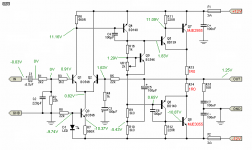
p3a-f1_volts_shorted.PNG
I will now proceed to short the point between R1 and R3 to ground and take new measurements.
EDIT: The results are in and I still can't make any sense of it.
EDIT2: I noticed you asked about my bias voltage. My trimpot is set to middle, so VR1 = 1k at the moment. Collector of Q8 is at 1.27V and collector of Q7 is 1.76V.
p3a-f1_volts_shorted.PNG
Attachments
Last edited:
Hi,
the voltages around R1 to 3 should all be -ve. The emitters of q1&2 should also be -ve. Something weird.
Vled ~1.9V Vr7 ~1.2V, Ir8 9.94V
ILED ~0.45mA, far too low, Ir7 ~2.1mA, Ir6 ~1.25mA, leaves ~0.9mA through Q2
Ir10~2mA, too low
Vbeq4~700mV, too high for a 2mA Ic.
It could be that the artificially low supply rails are not biasing the VAS to design current that the voltages don't appear right. That's one of the downsides to VAS fed with resistors. Very intolerant of varying rail voltages.
But, that does not explain the +ve voltages around the input???
I wonder if Q1 is dead?
Gah, AndrewT was right indeed. Replaced Q1 with some BC546 I found lying around, currently nicely 0V at output. However, the one I removed was brand new when installed and when I measure it right now with multimeter it looks perfect - it's like two diodes with ~800mV voltage drop. Seriously confused. (anyone have ideas how to perform more tests to see what the devil was up with that?)
I will continue with testing and will keep you posted.
Thanks a lot for all your help, guys!
I will continue with testing and will keep you posted.
Thanks a lot for all your help, guys!
Well, there's your problem! hFE = 4. However, if I reverse the leads hFE=245.
According to all datasheets I have seen, BC547 should have emitter on the right side when facing labels. I measured all of the transistors I had in this batch (12 of them) and 11 had emitter on the LEFT and hFE around 245-255. One of them had the emitter on the right and hFE=435!!!. They are all Fairchild's BC547B's. Possibly fake?
According to all datasheets I have seen, BC547 should have emitter on the right side when facing labels. I measured all of the transistors I had in this batch (12 of them) and 11 had emitter on the LEFT and hFE around 245-255. One of them had the emitter on the right and hFE=435!!!. They are all Fairchild's BC547B's. Possibly fake?
That's a real problem. With heatsinks about 5% of required rating, it will soon be toast with any kind of output transistorThe MJE3055 & MJE2955 heatspreaders are way too small , even with +-12V supply voltage , Q9 should be in thermal contact with one of the heatspreaders.

Actually, as Sakis has demonstrated, placing the bias transistor alongside or on a driver transistor gives a better tempco and safety for P3a CFP design.
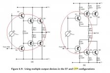
the P3a has a CFP output stage.
The temperature compensation should not be fitted to the output devices. The temperature compensation must be fitted to the two driver devices.
Placing all three in a row and coupling them to a strip of copper ot aluminium should be sufficient.
A CFP output stage can run with very low crossover distortion with as little as 5mA of output bias current. The drivers could have a similar bias current, but more usually a bit less (2mA to 3mA the same as in the sch.) for a total output Pq of 120mW @ +-12Vdc. The driver Pq total is ~70mW
The heatsinks on the output devices are perfectly adequate for +-12Vdc and music reproduction during testing.
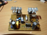
Currently I can't complain about insufficient cooling. However this is because I am trying to end up with an amp that runs off of 13.8V - I made the power supply quite poorly (whipped something up quickly) and it heats up a lot more than the amp (as a sidenote, amp and power supply each have a fan blowing on them (2 fans!)). Apparently the part that heats up the most in the PSU is the transformer. Probably unsuitable amount of turns for that specific operating frequency. But this is not exactly a talk fitted for this sub-forum anyway. When I get more spare time I may rebuild the PSU and try to do it properly this time.
Actually, as Sakis has demonstrated, placing the bias transistor alongside or on a driver transistor gives a better tempco and safety for P3a CFP design.
If the drivers heatspreaders are little enough such that their
temp is higher than the one of the power devices heatspreader
sure that it will work better....
But not in the particular case of the amp above, isnt it ?...
I take the point that this driver stage needs no heat spreader at all. However the tiny output transistor spreaders fitted will likely cycle wildly and indeoendently in temperature and the bias with it. Fan cooling will add to the variables. I would seriously rethink the assembly, parts and compensation arrangements for the OP 50-100W version that surely should be the model for this test assembly.......But not in the particular case of the amp above, isnt it ?...
Sensing the output transistors is notorious for problems with unsuitable tempco on CFP designs. It's a matter of the slope which only need compensate for half the number of junctions of an EF2 design, where the drivers are forced to track the main heatsink temp. The problems were evident with commercial products and it is better, I think, to go with the designer's scheme for DIY builds. According to D. Self also, the drivers are the way to go, and just one driver transistor and tiny spreader may be sufficient here. Further, I can't see that it's necessary to use both devices to provide the same information - unless the notion of symmetry is more important.
Interesting, I'm new to Audio, but I agree with what I think I understand
from what AndrewT is saying.
From the attached drawing, It seems that EF output amp bias is affected by Drivers, but mainly heavier biased and warmer final outputs.
Its my opinion from looking at the circuit,
am I must state again, I don't have experience in this, so its only an opinion,
That the CFP output's bias is mainly influenced by the temperature differential of the driver pair, at least for bias transistor to be in thermal contact with drivers.
Regards
Attachments
All the output devices change temperature from start up to warmed up quiescent to hot just after a high power series of transients.
Theoretically all these Vbes need temperature compensation.
From what I recall Self said that the the outputs of a CFP stage required only 1/6 of the tempco compared to the drivers. He and most others choose to ignore this small tempco requirement and concentrate their efforts and the very much needed tempco of the drivers.
I have a couple of amplifiers where the two drivers and the Vbe mulltiplier, All To92 devices are attached to a common heatsink. These two designers appeared to have agreed with Self's observation.
On that basis, the CFP on the right is correctly shown with the tempco around the Vbe + drivers.
- Status
- This old topic is closed. If you want to reopen this topic, contact a moderator using the "Report Post" button.
- Home
- Amplifiers
- Solid State
- P3A problem - DC at output