LSK389B is used in a cascoded LTP and the working points are set, the tail current of the LTP to 11.3mA and the source to drain valtage to 4V. Are those good working points or the voltage should be set to 10V? Simulation does not show much improvements. Idss for B type is 6 to 12 mA. Idss for C type is 10 to 20 mA, what is optimal bias current for C type.
Continuous power dissipation for LSK389 is 400mW/125 degree.
dado
Continuous power dissipation for LSK389 is 400mW/125 degree.
dado
LSK389B is used in a cascoded LTP and the working points are set, the tail current of the LTP to 11.3mA and the source to drain valtage to 4V. Are those good working points or the voltage should be set to 10V? Simulation does not show much improvements. Idss for B type is 6 to 12 mA. Idss for C type is 10 to 20 mA, what is optimal bias current for C type.
I will treat the Vds operating point used by manufacturer to measure other parameters (such as trans-conductance) as the minimum. For K389 it is 10V. Real implementation is based on the whole circuit or topology, but I don't want to go lower than 10V, unless there is new ideas in a "new" topology where more benefit can be achieved with that approach.
Once the Vds is above 10V, I believe the bottleneck is in the preceding stage, so the actual/chosen Vds will vary depends on the design/topology.
In most high rail circuit, cascode is a must to limit Vds. And this cascode imo presents more problems than the JFET itself. There are many circuits with BJT input where similar cascode is used. I think that is wrong (Even with JFET input, when maximum Vds is so high, I will not use the cascode).
OPTIMAL BIAS CURRENT. I think the situation is also the same here. The JFET wants a high current, that's true, but the circuit is not single stage design. Meaning that you have to consider what is wanted by the whole circuit. Usually lower bias current will work better for common topology in class AB (It will allow for easy access to wide bandwidth amp, etc etc).
With your setup, I can see that you are trying to get the most out of the input stage. The question is, can you work out the preceding stages to get a good whole result? It is about compromise. I believe you have studied the Roender's FC100.
In most high rail circuit, cascode is a must to limit Vds. And this cascode imo presents more problems than the JFET itself. There are many circuits with BJT input where similar cascode is used. I think that is wrong (Even with JFET input, when maximum Vds is so high, I will not use the cascode).
What would you suggest to use instead the cascode?
What would you suggest to use instead the cascode?
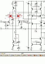
No, what I mean is, there are schematics where the input bjt can get away without cascade (for example in bjt input where Vce max is high enough) but the designer put the cascade there. I may use wrong terminology here (the cascade) but the cascade I'm talking about is the one to limit Vce or Vds to within its SOA. I prefer the signal direct from input to VAS. Attached is an example of the cascade I'm talking about.
Attachments
The cascode may not be strictly necessary from an operating voltage POV, but as shown it neatly eliminates Early voltage related common-mode distortion plus nonlinear input capacitance related input impedance distortion. While a low-level, high-gain application like a phonopre is unlikely to benefit (well, maybe towards the high end of the frequency range, though the source would be expected to be far worse), I would definitely include one in a line-level or power stage.
Last edited:
- Status
- This old topic is closed. If you want to reopen this topic, contact a moderator using the "Report Post" button.