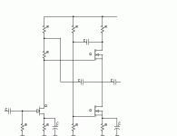
Hi all guy´s. I´m planning to make a test of a White Source Follower using small BS170/107/2N7000 Depletion mode MOSFET´s. Did anybody make such a circuit?
I´ll drive it with a BF245 JFET and the drain load resistor bootstrapped from the output of the WSF.
Ideas, suggestions???
I´ll drive it with a BF245 JFET and the drain load resistor bootstrapped from the output of the WSF.
Ideas, suggestions???
Attachments
Last edited:
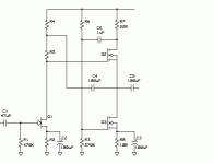
The OSF
Finally I did a test circuit with the WCF, implemented around two MOSFET´s, and results are satisfactory.
The circuit was made trial and error, no calculae, but in the future I´ll do it in the wright form.
I made two versions, both of them similar results. One of them uses US transistors: MPF102 for Q1 and 2N6661 for Q2 and Q3, and the other, japanese ones, with 2SK117 and 2SK2962 respectively. Resistors not labeled varies from one to other: R2 is 2.2k for US, and 3.9 for J. R6 is 1M for Japanese, and 680K for US transistors. Finally, R4 and R5 are 6K8 and 3.9K for US, and 10K and 6K8 for J. Both was adjusted for maximum output swing, about 6.8Vpp for a 12V supply over a 32R speaker from old color TV, and for minimum distortion. As the test were made on a plug in protoboard, and capacitances are high, some HF oscillation is viewed in negative peaks. Removing C4 (bootstrapping), gain is 5 times from input to output with load connected, and with c4 in circuit, gain is about 10 times greater (50 in total).
Then, I called it "The OSF", an acronym of Osvaldo Source Follower, ja ja ja...
Attachments
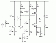
More in my OSF
Hi all. The past weekend I was upgrading my OSF, and I added some components to make a mix of the "augmented cathode follower" plus the "White cathode follower", but in solid state all-FET devices. I can tell that it is working pretty fine. This is the circuit:
The circuit is a mix of a "Augmented Cathode Follower" plus a "White Cathode Follower" but with all-FET stages.
Components not specified are: Q1 and Q2, 2 units of 2SK117 or 2SK150A. R4 depends on the transistor chosen, and is 2.2K for 2SK150 and 3.9K for 2SK117.
Q3 and Q4 are 2SK2692. DC voltage at output middle point is about 5V for a 12V supply. Quiescent current in Q3/4 is about 30mA and gives about 8.4Vpp over a 32 ohms load, and a AVf of 19 times (R8/R9 +1).
It has two bootstrapping loops, C3 is for increased gain and lower distortion (not measured, just saw the output in an oscilloscope), and C2 to increased input impedance.
The output coupling to load is a bit strange, but I like this way of wiring. Can be used a cap from middle point to a grounded load, and other from GND to +B, as ussualy.
Regards.
Attachments
 I like it
I´m designing it as the audio output for a AM portable regenerative receiver with the only FET stages, no opamp, no BJT´s at all. It is doing its job satisfactorily.

you should get very good sound quality even from cd or different good source.
C2 caused problems in my simulations, I had to remove it
- Status
- This old topic is closed. If you want to reopen this topic, contact a moderator using the "Report Post" button.
- Home
- Amplifiers
- Solid State
- WSF and DMOSFET´s